1.2 GHz Fixed-Frequency Clock-Multiplying Digitally Controlled PLL
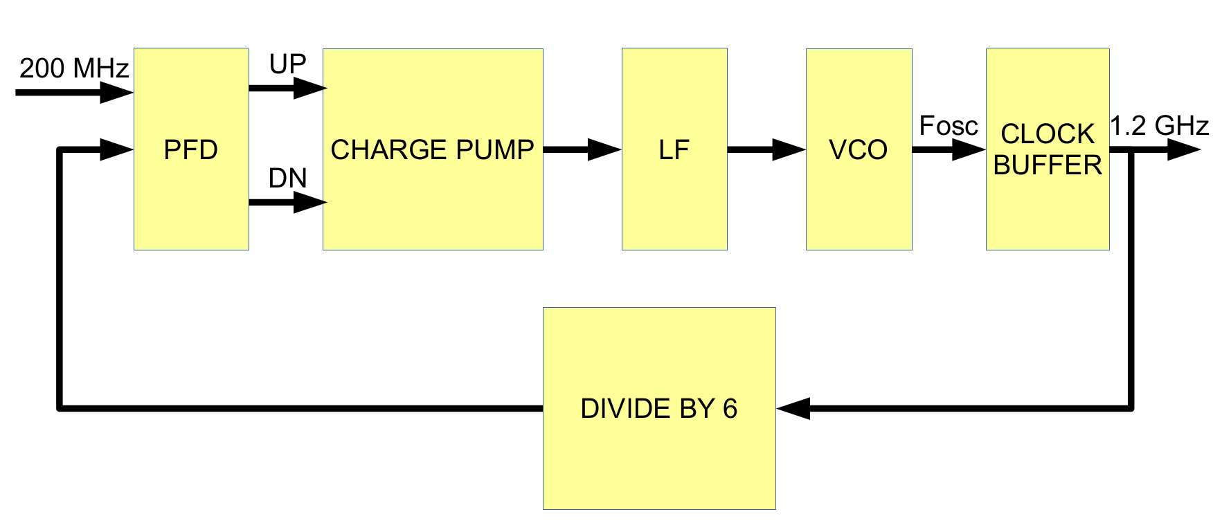
This PLL consists of Digital Phase Frequency Detector (PFD), Charge Pump, Loop Filter (LF), current-starved Voltage Controlled Oscillator (VCO), Clock Buffer and the Divide-by-6 Module.
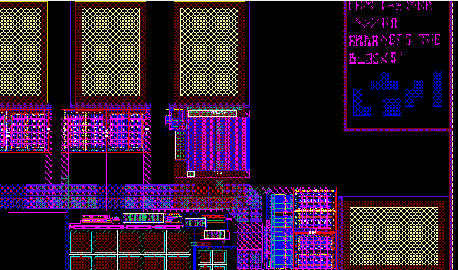
The layout is shown below, I decided to put it closer to my pad frame, near my cool logo ;]
And the block diagram is here.
Phase Frequency Detector (PFD)
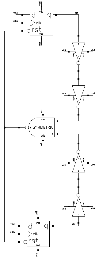
I implemented the PFD with two typical two-latch design flip-flops with asynchronous active-low reset and symmetric two-input NAND gate. The schematic is shown below
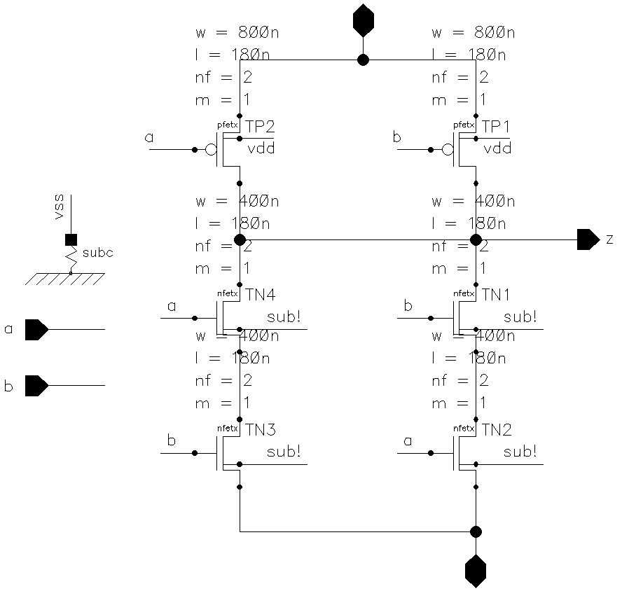
The important things to note here is that NAND2 gate must be symmetrical, fast and with equal rising and falling edges. That is why both if its inputs must have same parasitic capacitance. Below is the schematics of a NAND2 gate used in this design
I also added two inverters at the output of each flip-flop in order to make sure that they get reset only after their output is a stable logic HIGH. The inverters I used provide the necessary delay to achieve that.
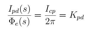
When PLL is in lock condition, the combined transfer function of PFD and the Charge Pump is
Charge Pump
The purpose of Charge Pump is to provide the output current depending on the duration of UP and DN signals. The basic Charge Pump is shown below
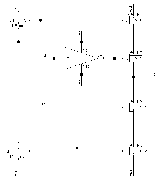
This charge pump sucks. The issue is the charge sharing from the switch transistors which messes up the voltage level at ipd node. If the TP9 is turned off after being initially ON, the gate oxide charge is injected both to its source and drain, and part of the charge injected to the drain changes the voltage at the ipd node.
I used different implementation, Maneatis, Ching. The schematics is shown below
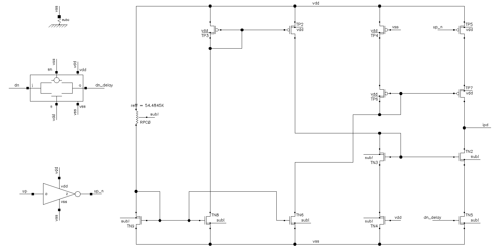
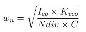
The switch transistors TP5 and TN5 are now connected to the node ipd through the mirror transistors TP7 and TN2 . This way the effects of the charge sharing are significantly minimized. The enabled transmission gate was also added to equalise the inverter delay. The transistor sizing and the design was based on the following calculations


Loop Filter
Loop Filter is an important element in the PFD. In this design I used basic RC type loop filter with the following transfer function given the response from charge pump

Schematic is shown below
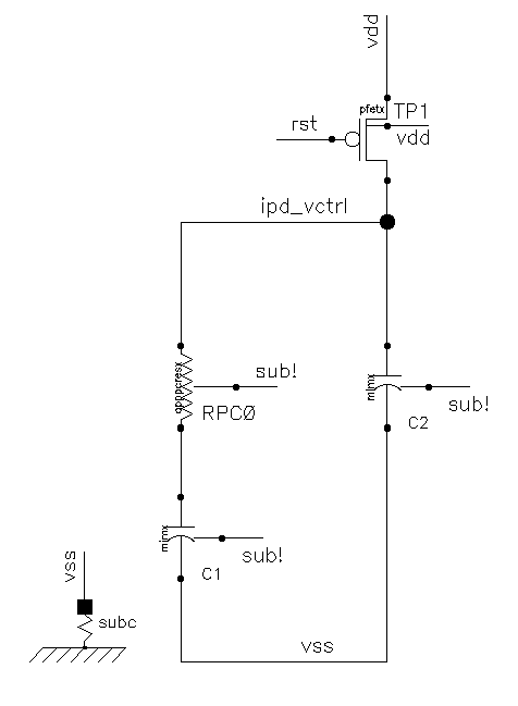
The PMOS transistor on top helps both to lock faster and to reduce the simulation time. C1 = 10 pF, C2 = 1 pF and RPC0 = 7.96 kOhm
Voltage Controlled Oscillator
The VCO used in this design is described here
Divide-by-6 Module
Below is a circuit for the divider

Clock Buffer
The Clock Buffer used in this design is described here
Simulation
Simulation was done for the main blocks and for the whole DPLL.
PFD and Charge Pump Simulation
Below is the testbench schematics
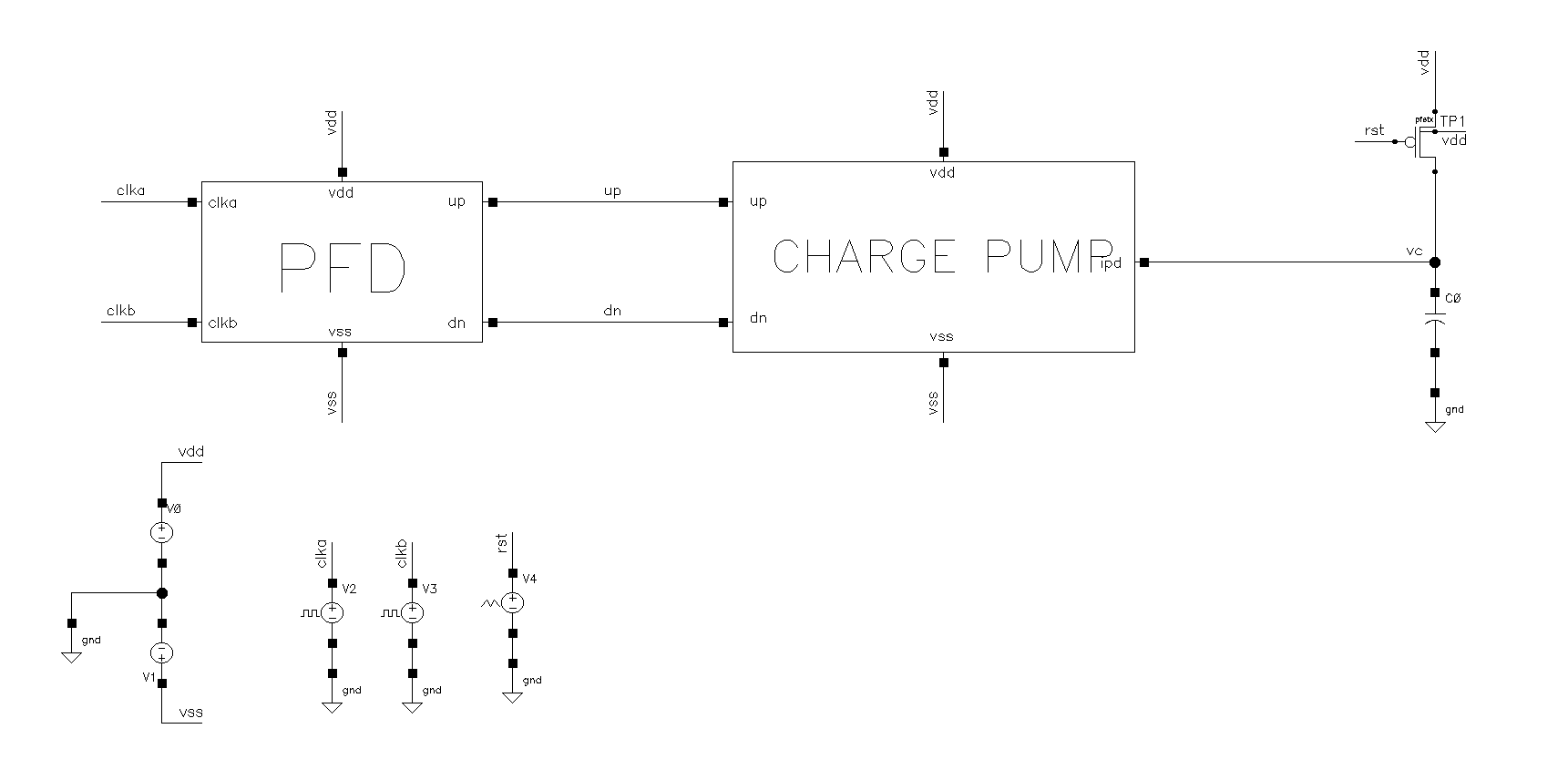
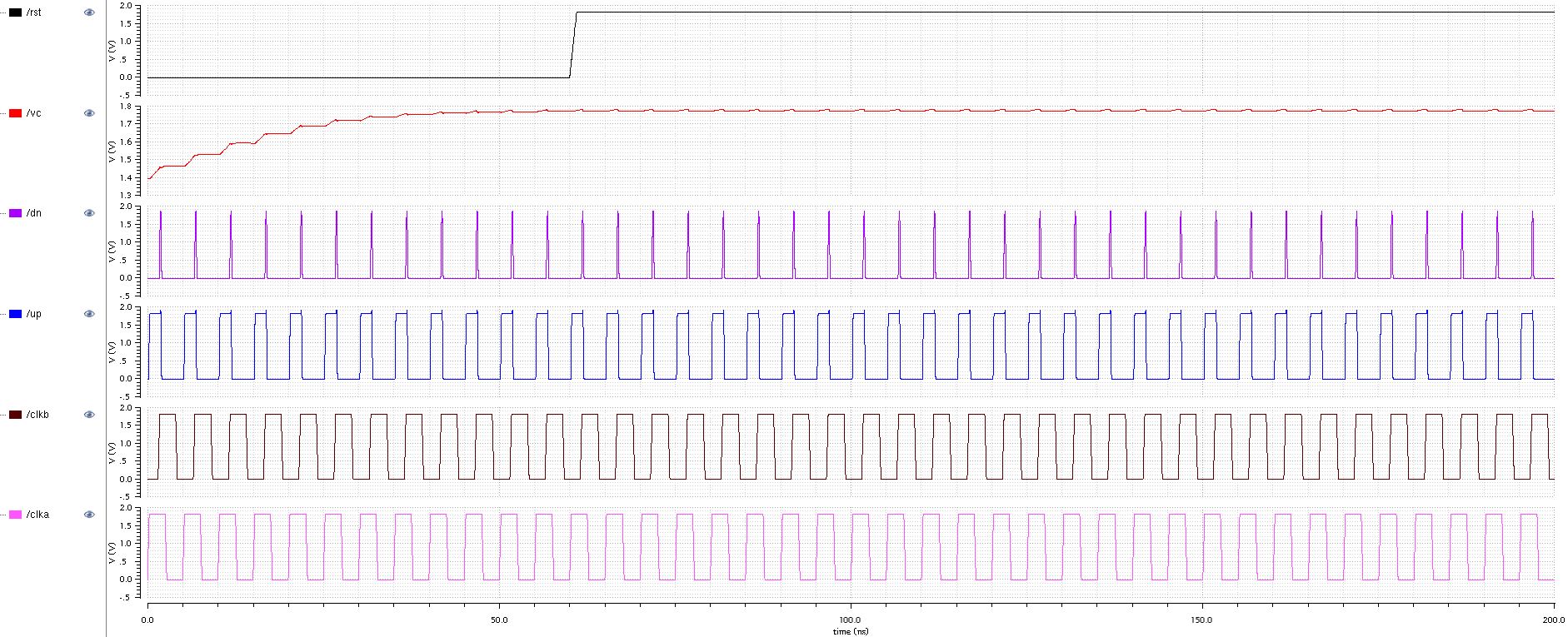
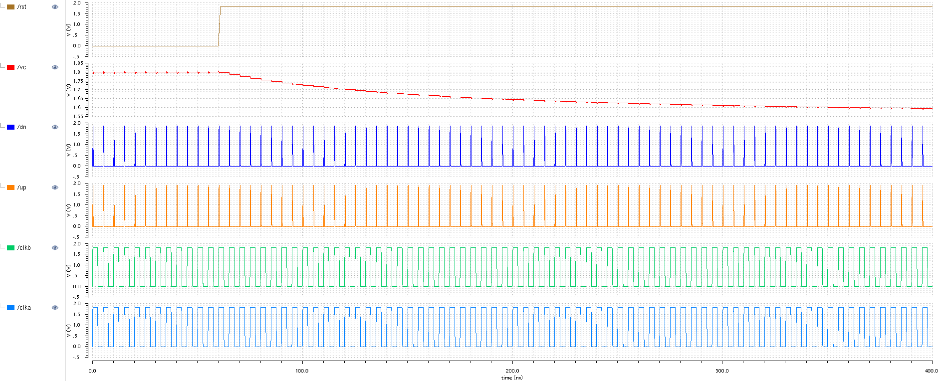
First I disconnected the reset transistor and set the clkb to be delayed by 1.5 ns. As a result, we can observe the output capacitor (with reduced value for simulation speedup) to be charged up to vdd and the UP signal is now much wider than DN signal.
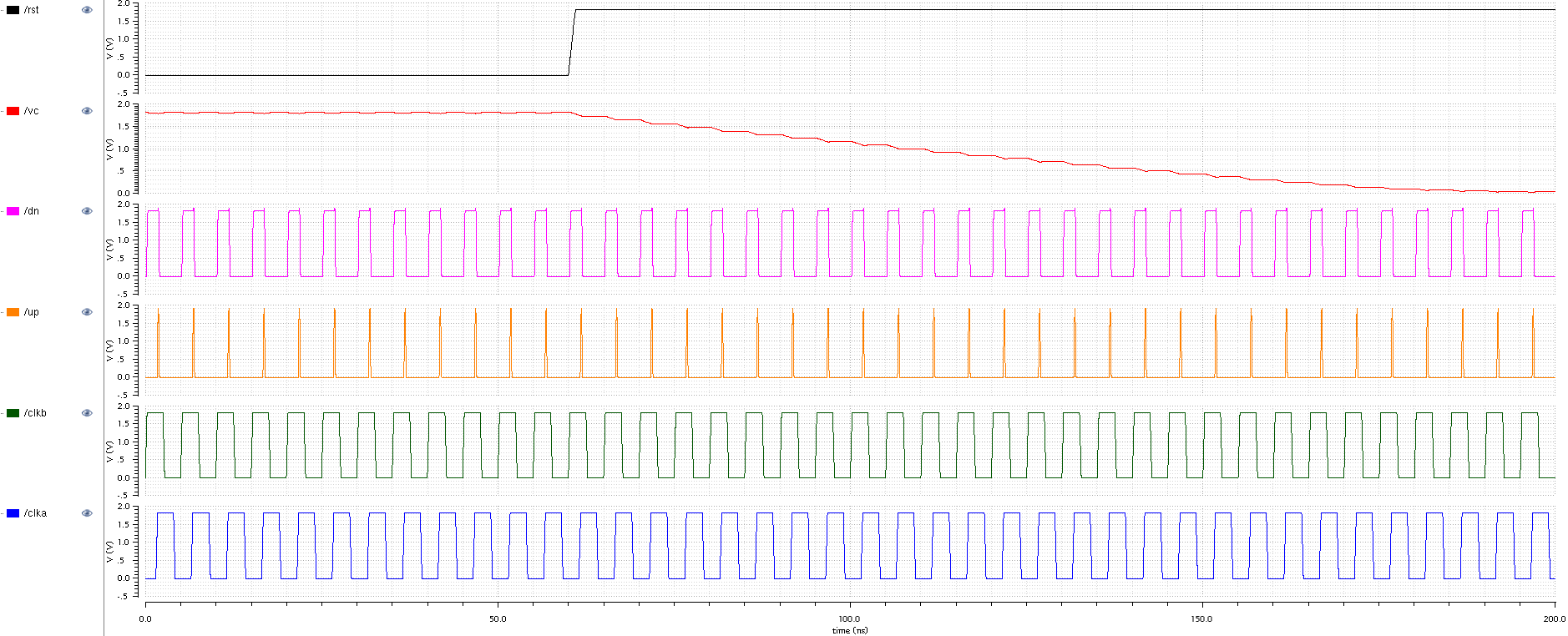
Now I connect back the reset transistor, and set now clka to be delayed by 1.5 ns. As a result, we see the voltage at the vc node going down and the DN pulse is now wider than UP pulse.
Now I make both clock sources to be perfectly in-phase. The voltage at node vc now settles to 1.6V and both UP and DN signals are in-phase and have almost similar duration.
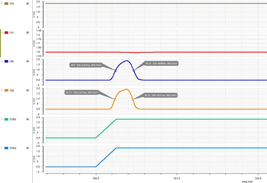
Here is just the zoomed plot of the previous simulation. The DN and UP signals are of course not perfectly same in duration, DN pulse is 224.6 ps wide and UP pulse is 222.8 ps wide.
DPLL Simulation
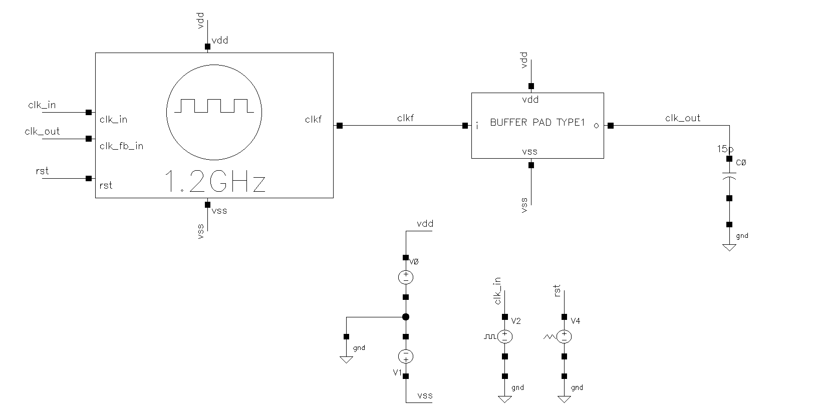
Now I can simulate the whole thing. Below is a testbench schematic
Below is a simulation plot
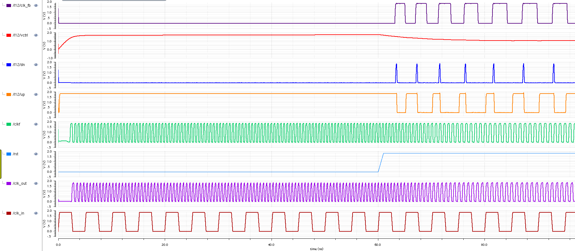
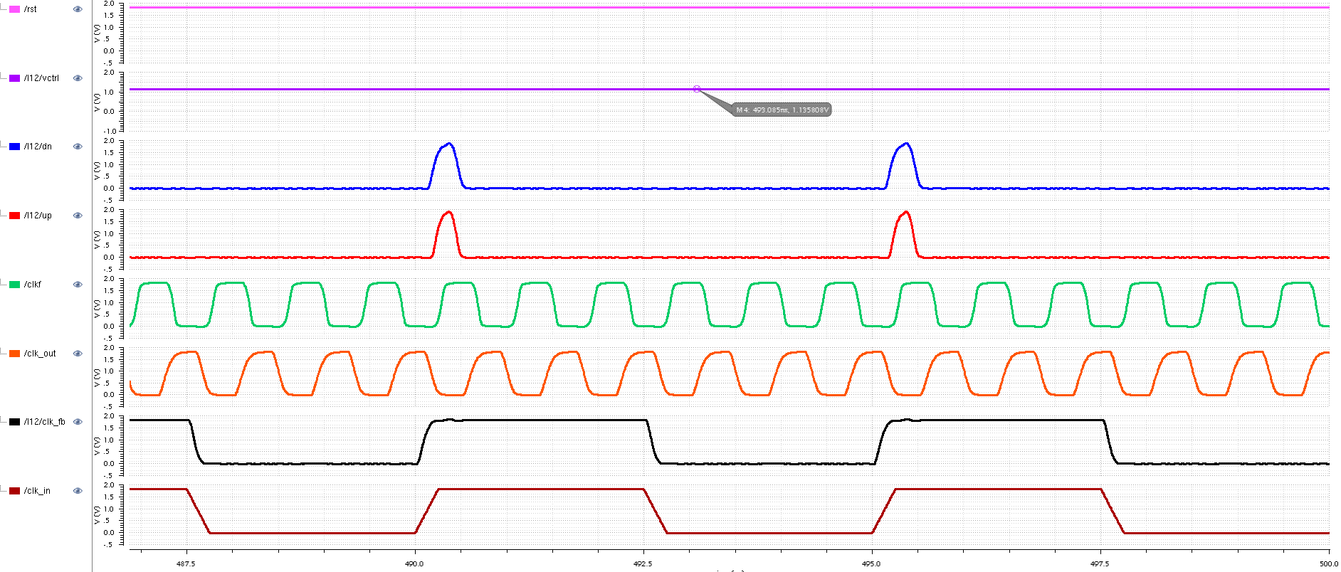
Here is a zoomed last 24 ns of simulation. The control voltage vctrl is settled to 1.135V the output clock signal clk_out has nice sharp edges given the 15 pF output load capacitance and a 50% duty cycle. The clk_in and clk_fb are nicely aligned in phase. So the DPLL seems to be working.
After that, a layout has been done and the chip was submitted to MOSIS fabrication.
Test PCB Design
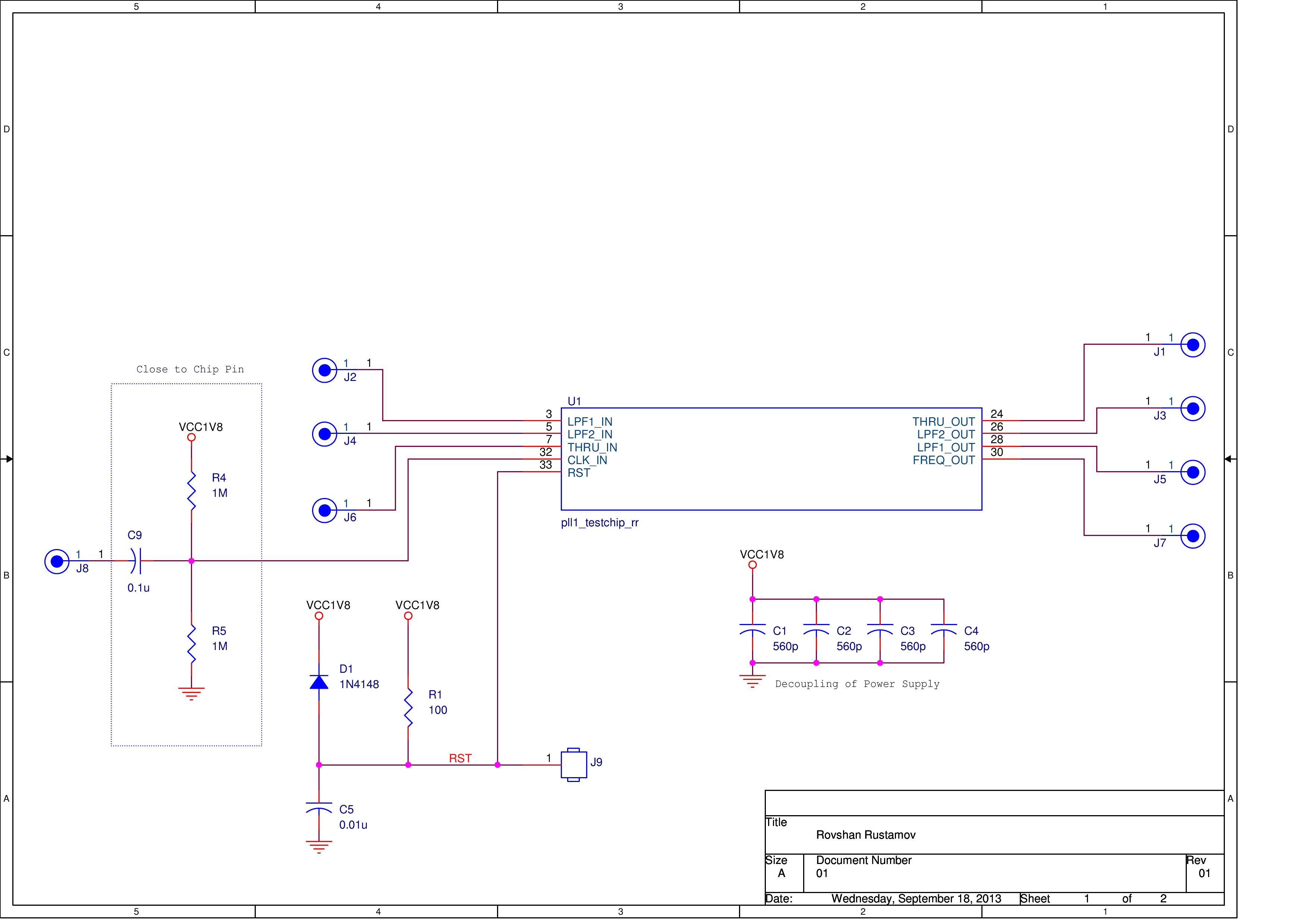
The test PCB schematics are shown below. The decoupling capacitors C1,C2,C3,C4 were selected so that to kill the 200 MHz input signal ringing into the supply line. The D1,C5 and R1 are forming the delay for the RST pin of DPLL. The C9,R4 and R5 are used for DC shifting the input sinusoid from signal generator which is centered at 0V.
The board will have some other IOs not related to this DPLL project. But the IOs related to this DPLL project are RST, CLK_IN and FREQ_OUT, and of course the supply and ground lines.
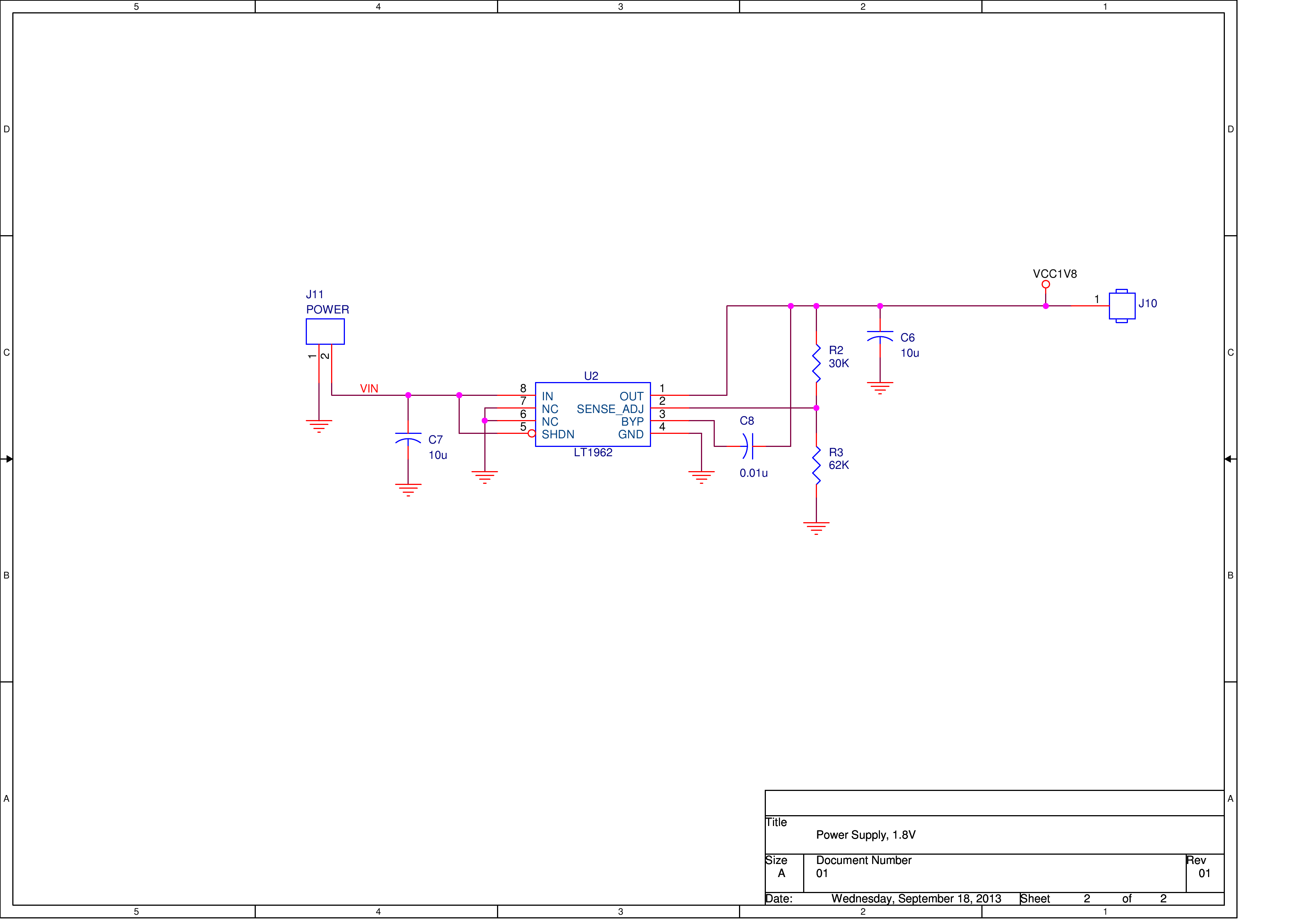
And this is just on-board LDO from Linear Technology
The PCB was made on the process described here.
Below is a picture of the finished PCB after the DPLL chip has been received and board has been designed, manufactured and assembled by me
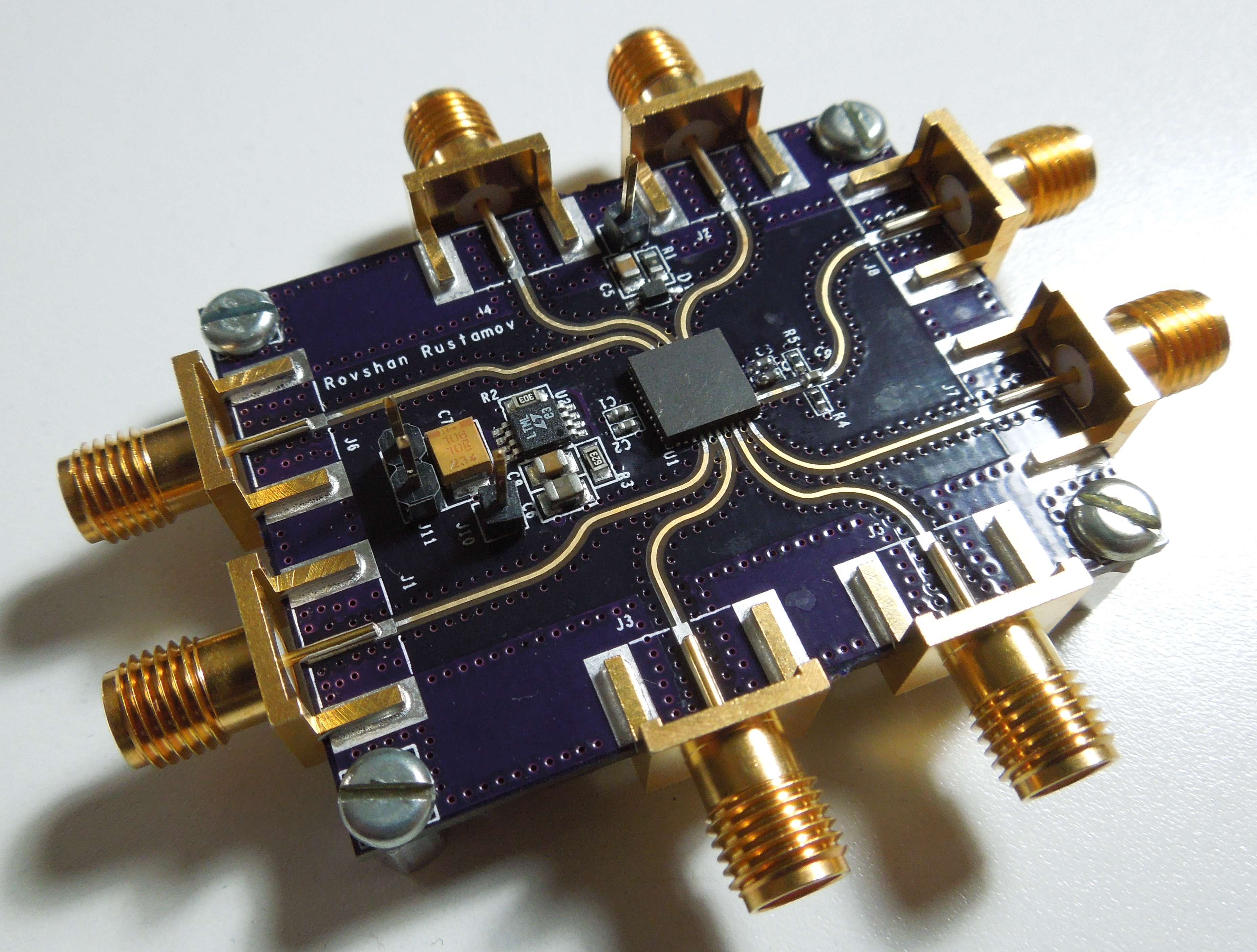
Looks neat? Of course it does! Okay, lets jump to testing.
References
J. G. Maneatis, "Low-jitter process-independent dll and pll based on self-biased techniques," IEEE JOURNAL OF SOLID-STATE CIRCUITS, vol. 31, no. 11, pp. 1723-1732, November. 1996.
Ching-Yuan Yang, Shen-Iuan Liu "A Wide-Range Delay-Locked Loop With a Fixed Latency of One Clock Cycle," IEEE JOURNAL OF SOLID-STATE CIRCUITS, vol. 37, no. 8, pp. 1021-1027, August. 2002.

