1.2 GHz Fixed-Frequency Clock-Multiplying Digitally Controlled PLL
General Measurement
It would be cool to see a time-domain waveform, however; I do not have a scope with > 1.2 GHz bandwidth to do that. But I have access to E4403B Spectrum Analyzer, so the first thing was to check the output of my DPLL chip with Spectrum Analyzer. Below is a snapshot
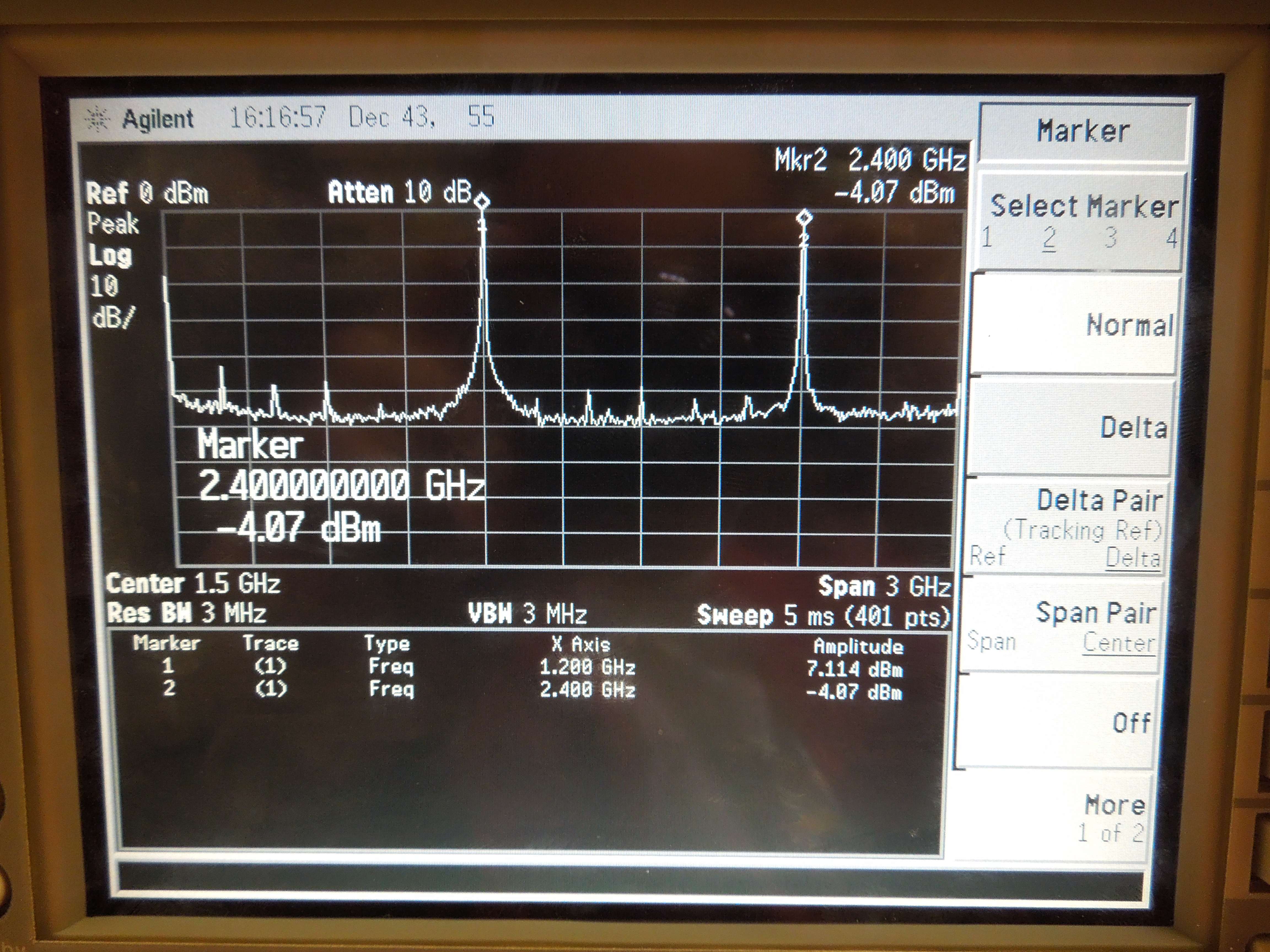
Okay, so I see the main peak right at 1.2 GHz with a signal power level of 7.1 dBm, not bad! It works.
Phase Noise Measurement
Next, I decided to get a rough approximation of the phase noise, so I took measurements of primary signal power level and offsets at different frequencies and then roughly approximated a phase noise using the following equations where example phase noise at offset of 1 kHz is calculated


Below go the measurement snapshots at offsets of 1 kHz, 10 kHz, 100 kHz, 1 MHz, 10 MHz, 100 MHz
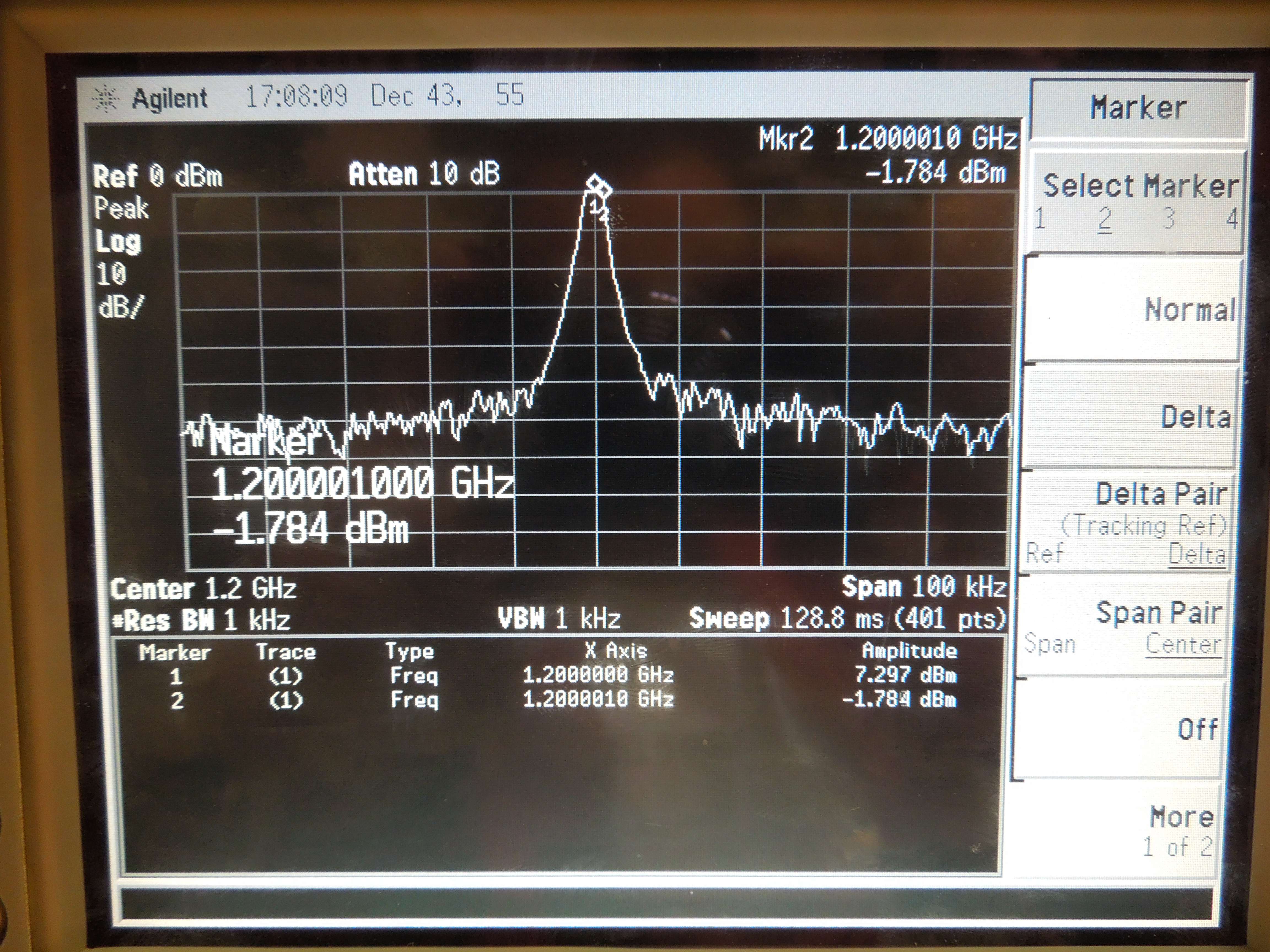
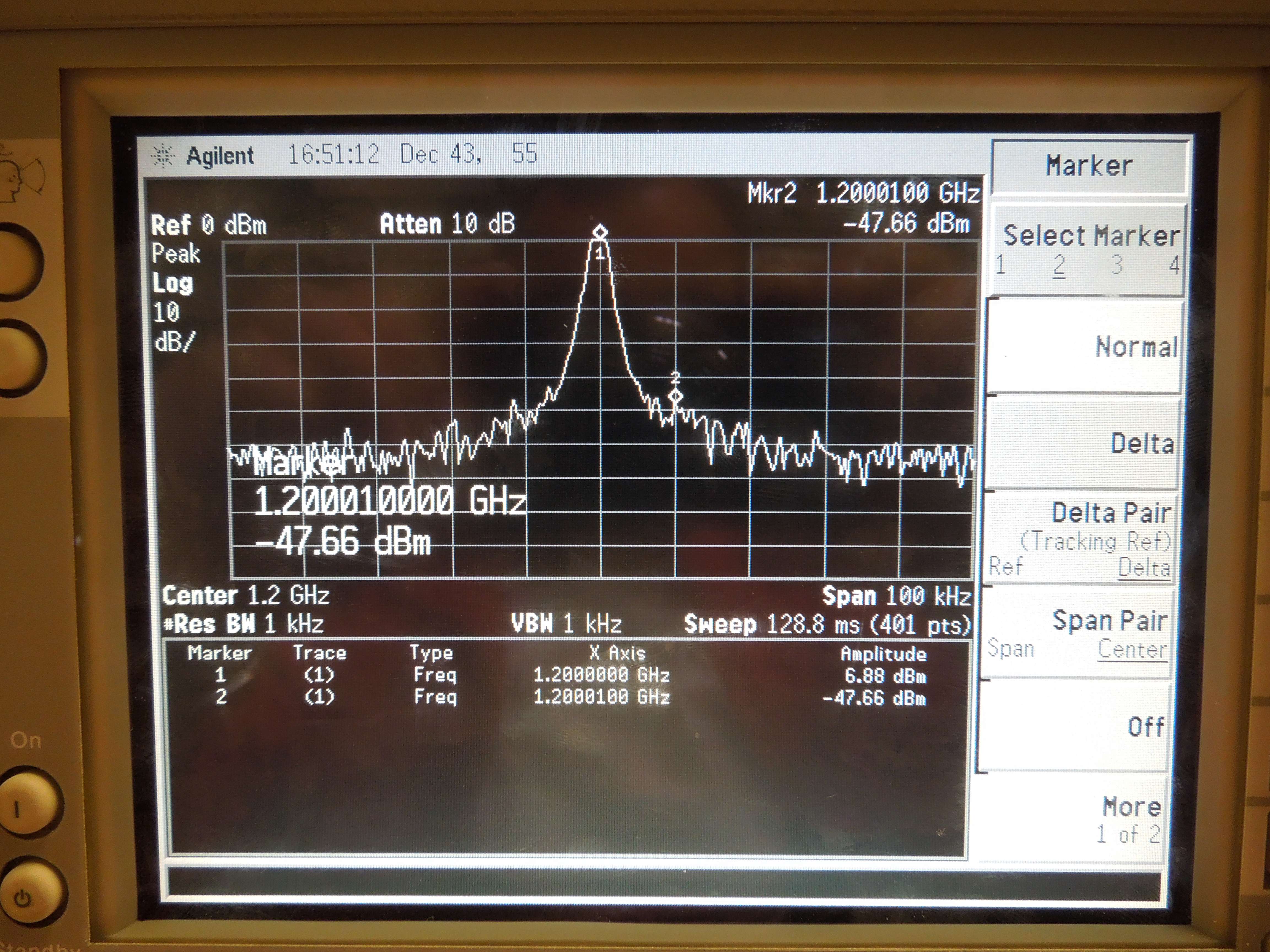
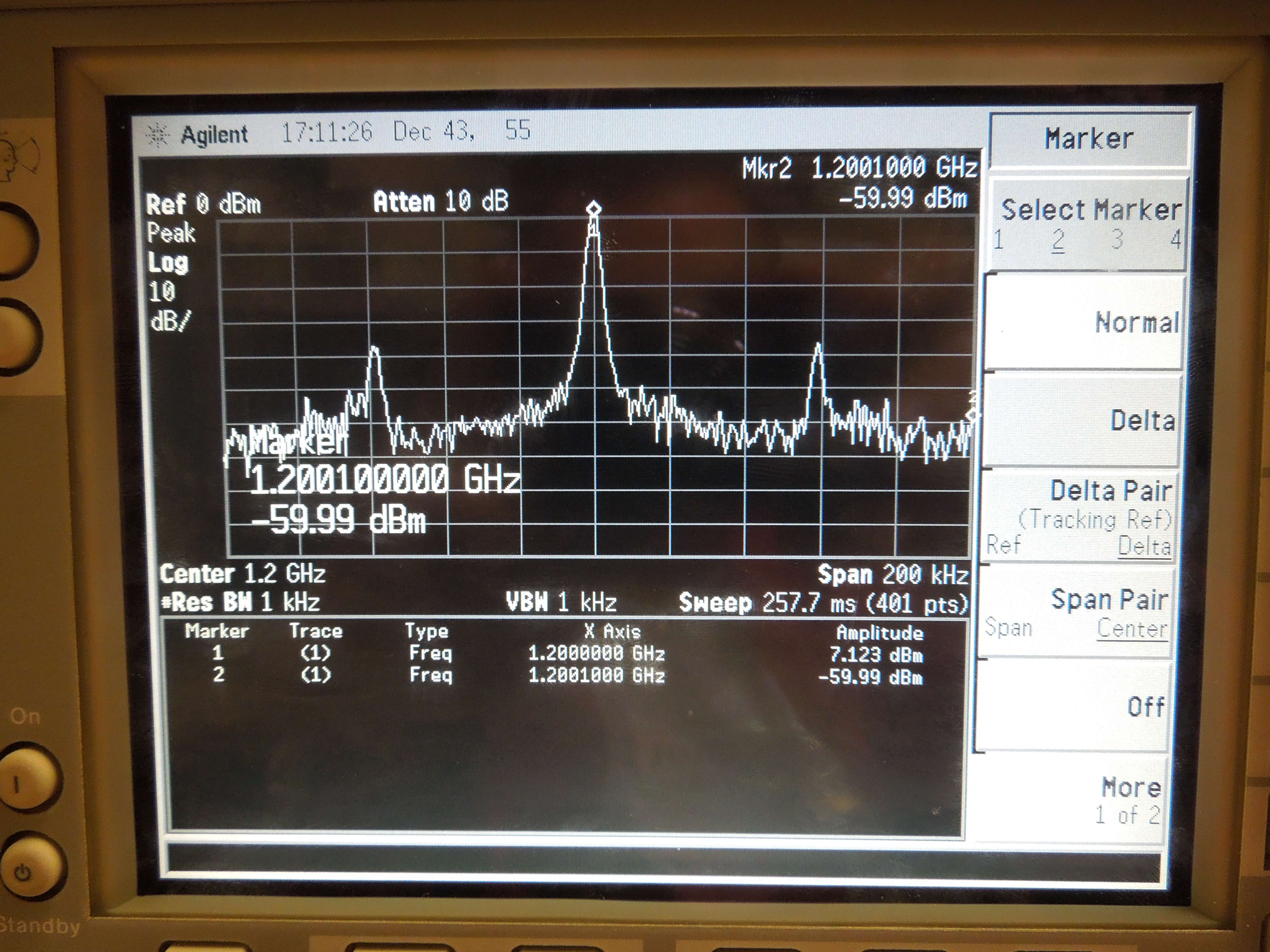
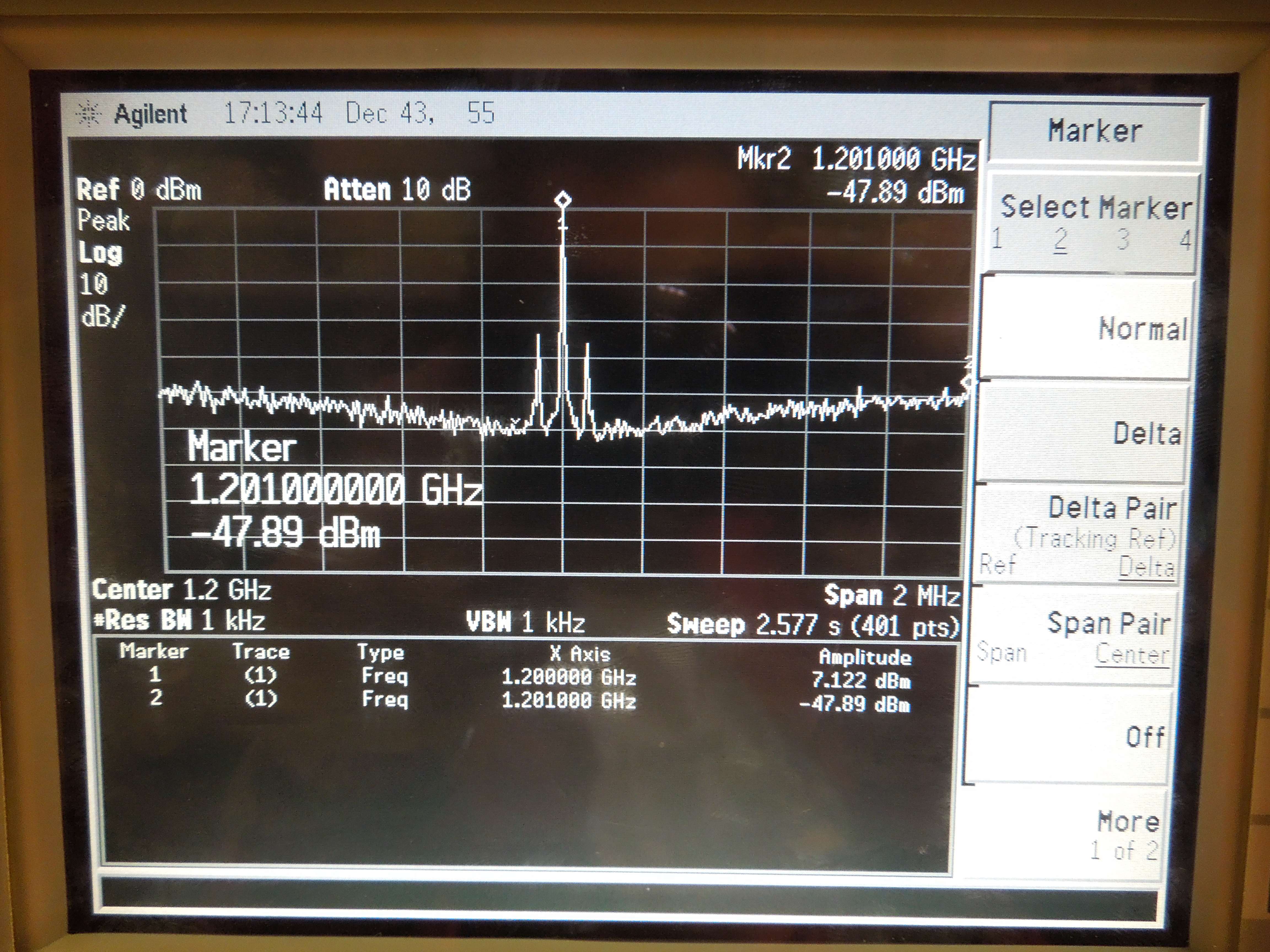
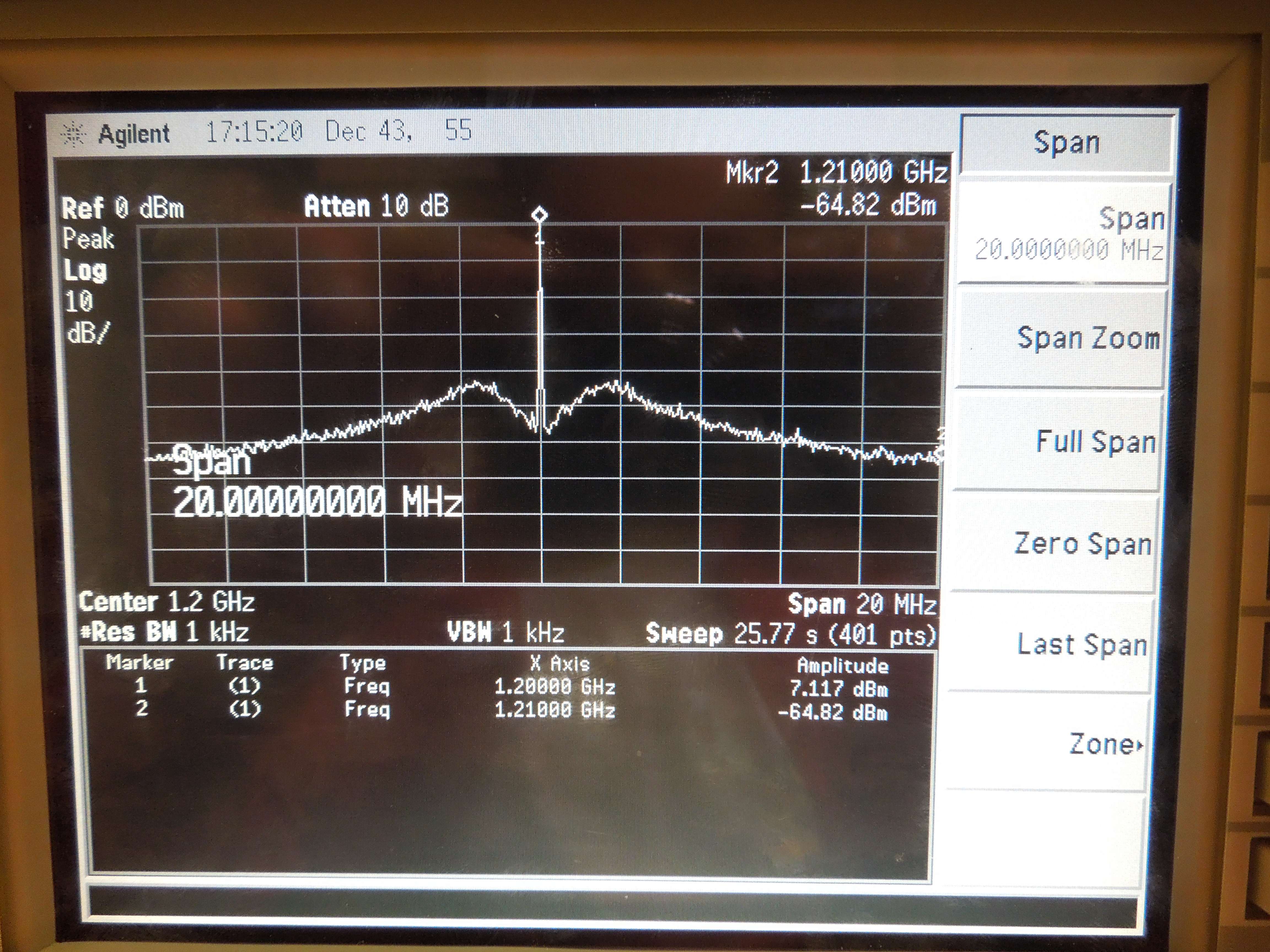
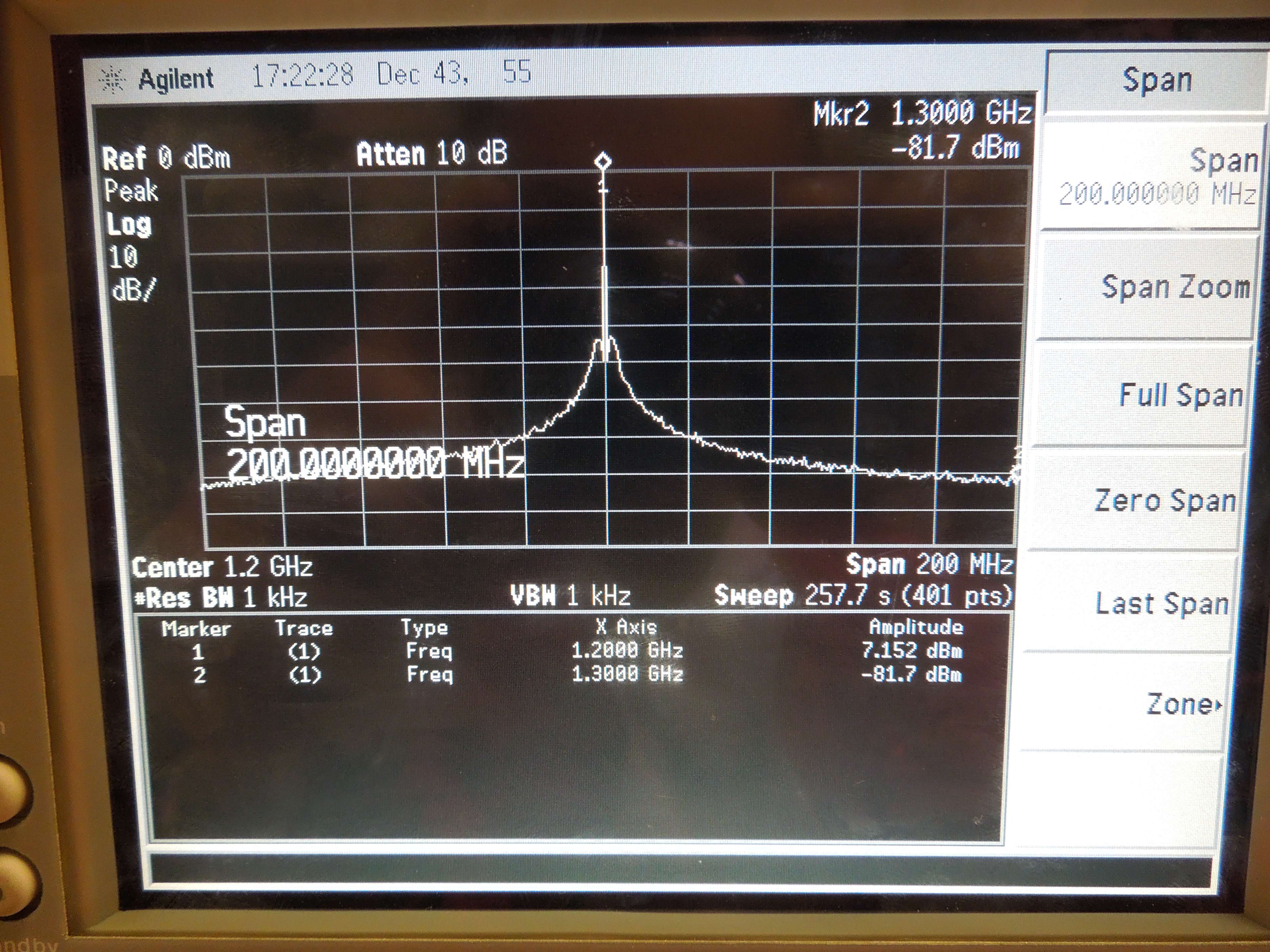
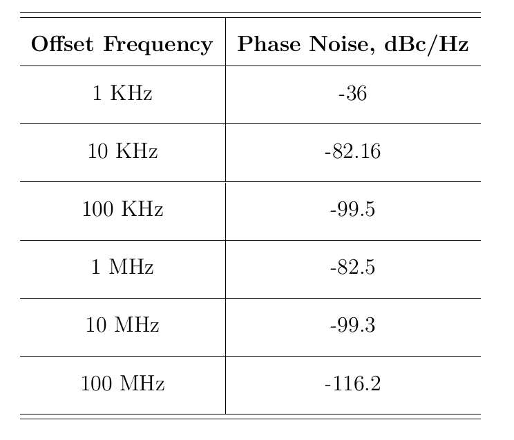
Below is a table showing the results of rough phase noise approximation for each snapshot
Time Jitter Approximation
Basically in order to know the Time Jitter, we need to integrate the phase noise measurement results. The concept is described in this Application Note from Analog Devices. There are already plenty of different spreadsheets and calculators available which automate process of phase noise measurement plot integration process, some of them are even available online, like JitterTime.
Using the above spreadsheet, the Time Jitter is computed as 52.88 ps. Note that if I were to use 10 kHz as the lowest frequency limit in the spreadsheet the jitter would be approximated as 18.8 ps. However, it is important to know that the smaller the lowest frequency offset limit of phase noise measurement used in integration, the more precise is the Time Jitter computation.
In any way, the Phase Noise and as a result a Time Jitter seem to be pretty high. Which makes sense for this design in which I used compact small but pretty noisy current-starved VCO based on five inverters. Those VCOs are really noisy, the good thing is that they are very compact, they do not require a lot of layout space. So, for applications where the Phase Noise or Time Jitter is not a concern this design is definitely a way to go. For applications such as, for example, clocking the high-fidelity, high-speed ADCs this would not be a right PLL to use.
Conclusions
I will be designing other types of PLLs, with completely different VCO as well as a different type of Charge Pump and Loop Filter specifically to achieve a lower phase noise. So, this was another successful design I rolled out with MOSIS on IBM 180nm CMRF7SF process.

