2 GHz Common-Source Low Noise Amplifier
DC Parameters Measurement
First I just powered it up and started looking at its DC parameters. The voltage of 1.8V was provided to the vdd supply and current through the biasing branch was adjusted to 8.5 mA. The current seen on the power supply rail was around 16 mA. That is much less than what I observed during a simulation, specifically 36 mA. So, right away I already see that from the DC point of view it behaves much differently.
I also decided then to check its DC behavior under various supply and biasing conditions. I performed 4 different measurements, and below are the supply voltages, bias currents and measured DC current through the supply line.
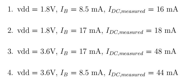
The measured DC current through the supply line is much smaller than the simulated currents.
It is important to note something. As you saw, I am using vdd of 3.6V, which is twice more than the process voltage of 1.8V, this is NOT something what one would do with a parts for series production. However, in my case, it is an experimental work and I am doing it just with few chips. My circuit consists also from a stacked transistors and I am also not exceeding the Vgs of each transistor above 2V. Given all that, it is "OK" to do it just for this experiment in order to better feel the behaviour of the circuit.
Measurement of Gain
At this stage, I decided to move on and see how the amplifier is actually working at a frequency of 2 GHz. I connected its input to the output of E4432B Agilent signal generator which was setup for output signal of -30 dBm at 2 GHz, and I connected output of the amplifier to the E4403B Spectrum Analyzer. The measurement plot is shown below
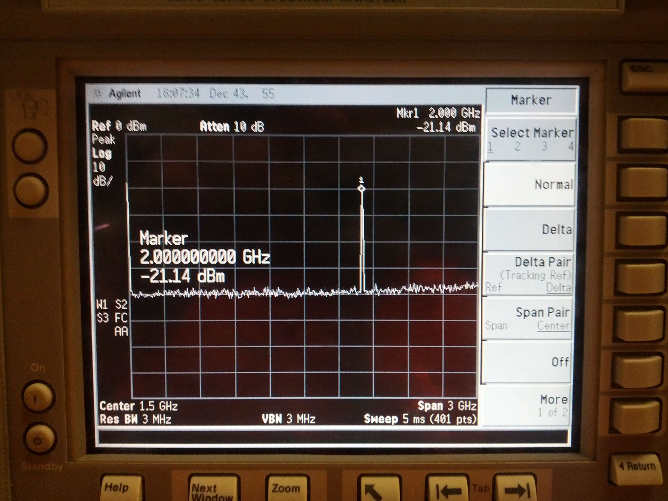
Alright, so the signal is measured to be around -21 dBm, that is by about 9 dB more than the signal provided to the input of LNA at 2 GHz. So, the amplifier is working. However, the measured gain of 9 dB is much smaller than the gain simulated which was around 23 dB.
S-Parameters Measurement
Next, I measured the S-parameters. The minimum power level at which I could perform measurement was around -5 dBm, which is way higher than the simulated input referred 1 dB compression point which was -19 dBm, however; I am suspecting that given the results of the above measurements the compression point might have moved up. So I will give it a try.
Below are S21 and S11 parameter measurement snapshots with epic reflective NA screen (usually I just write .s2p files to flash drive from NA, but this time just took a pic)
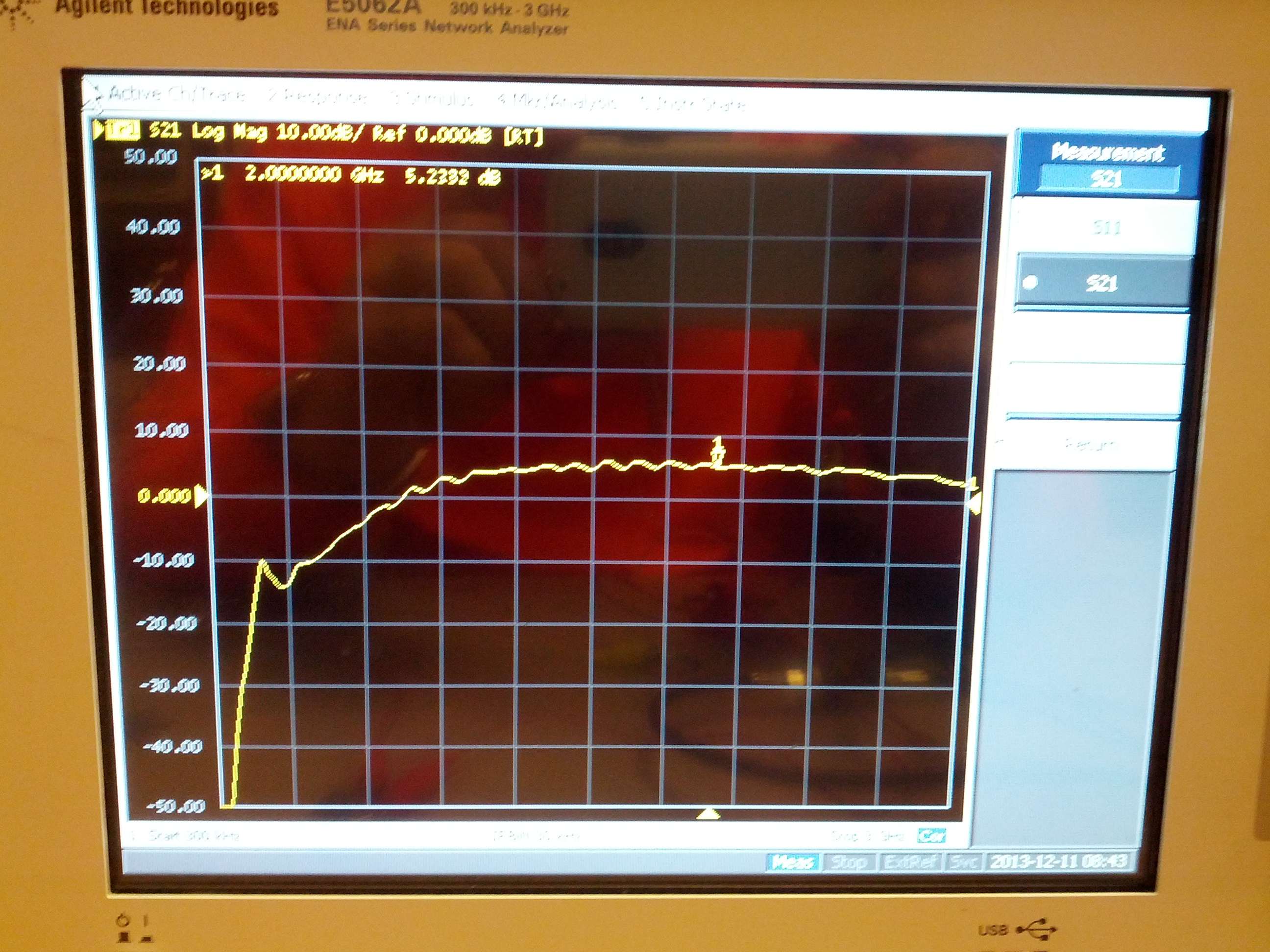
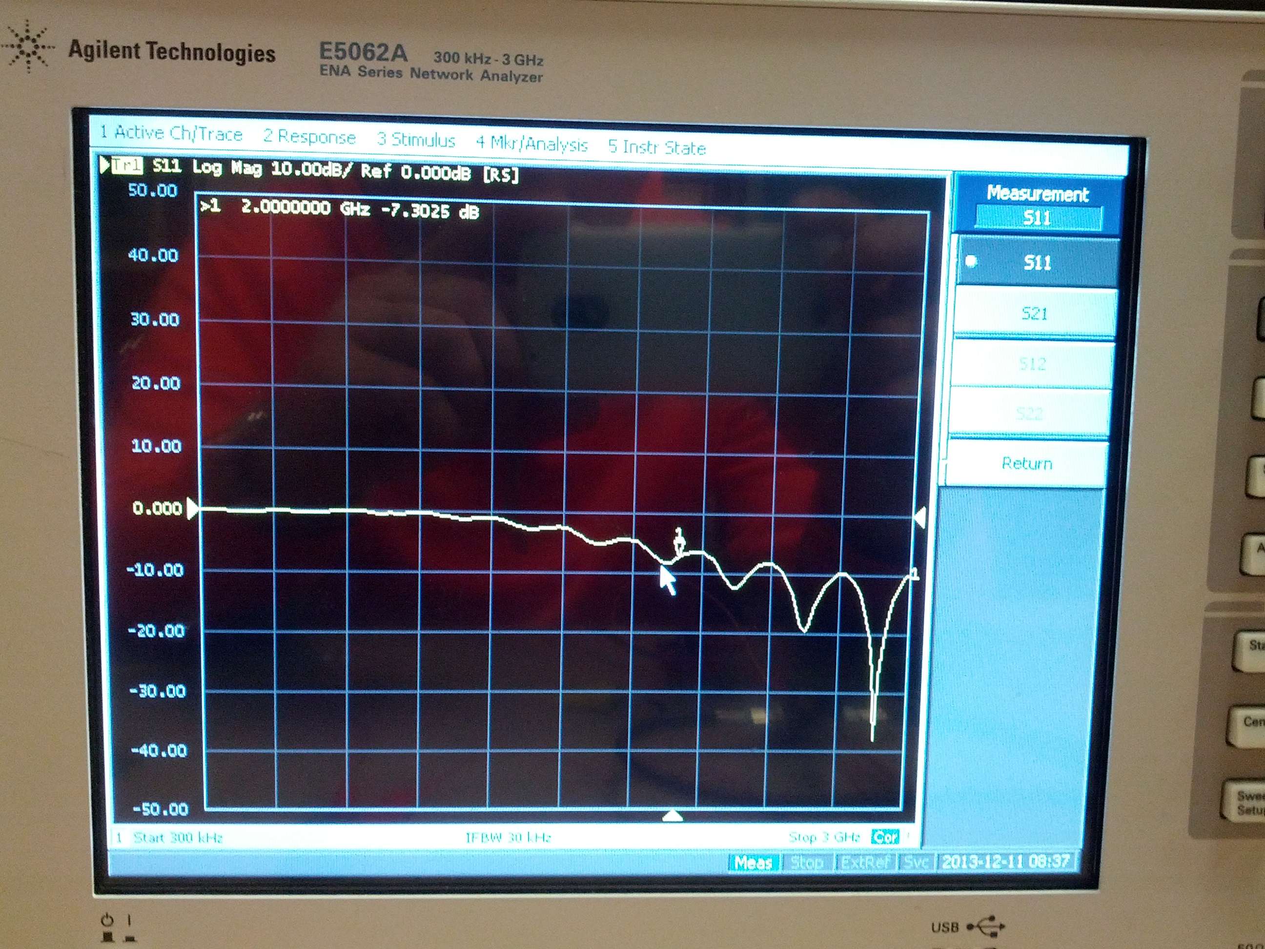
The first thing I norice is the measured gain to be around 5.2 dB at 2 GHz, not 9 dB as measured before with spectrum analyzer with -30 dBm input signal. So, I can conclude that 1 dB compression point is lower than -5 dBm. I will approximate it later.
Another thing I notice is S11 at around -7.3 dB.
Another thing I decided to do is now measure the S-parameters now at even higher power, 0 dBm, at that power the LNA would be driven more into compression. It is usually not necessary to do that, but I was just really curious to look at the measurement plots. So, below are again measurement snapshots of S21 and S11, this time with 0 dBm power used in Network Analyzer
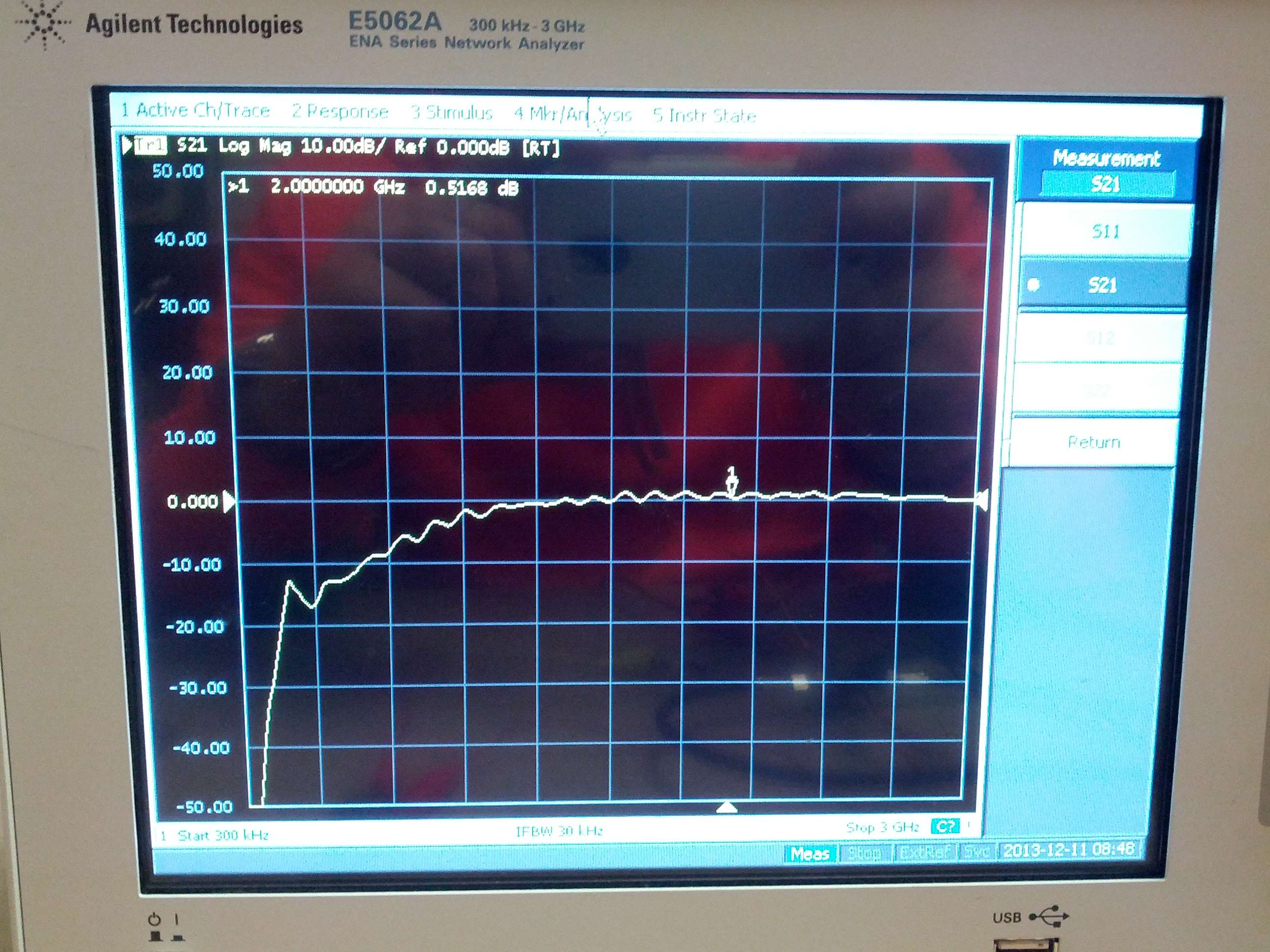
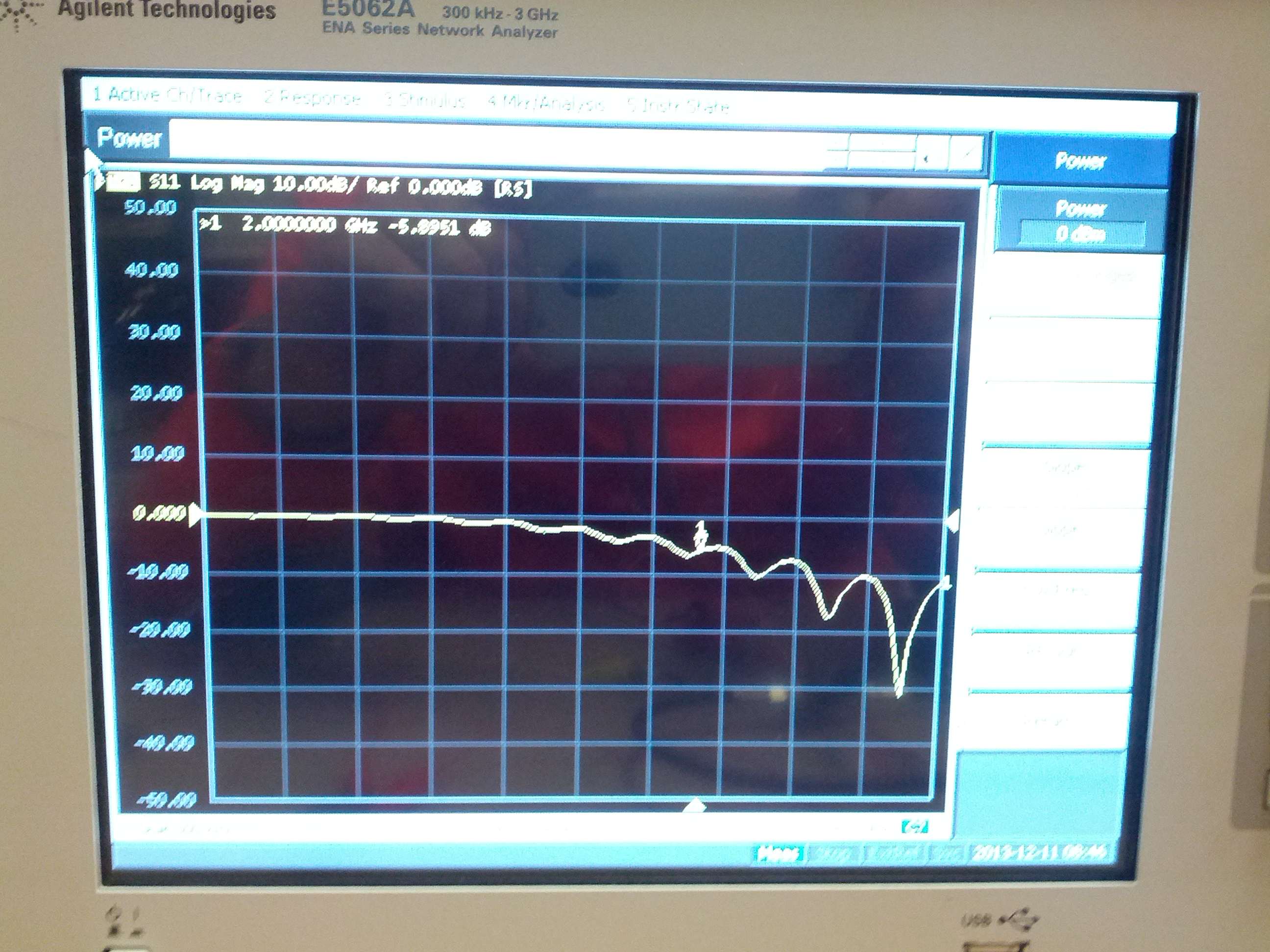
Now I see the gain dropped more, which makes sense since LNA is much more compressed now, S11 got a bit worse too.
Next thing I decided to do is to measure the S21 parameter at -5 dBm power when the LNA is supplied with 3.6V. Result is below
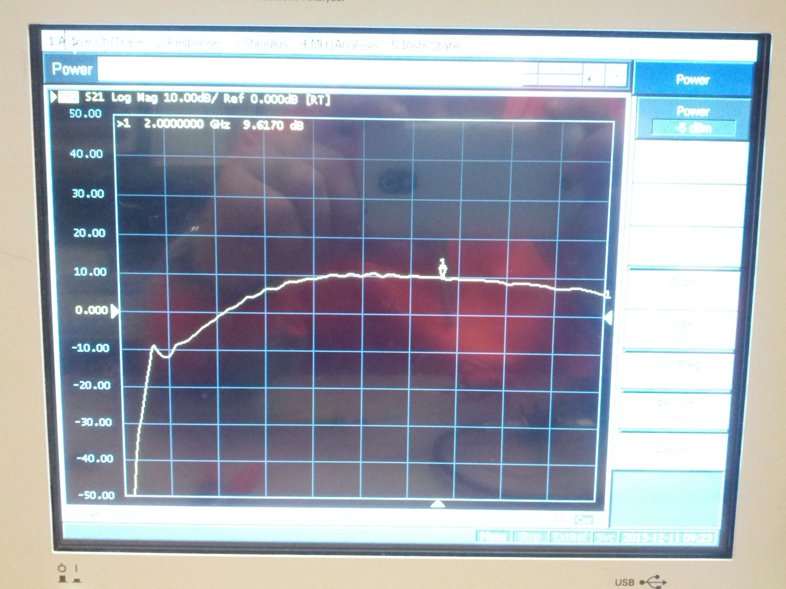
I see more gain now, 9.6 dB compared to 5.2 dB when the chip was supplied with 1.8V. Now I want to approximate its compression point. I will use signal generator and Spectrum Analyzer again to do that. Basically, I will just take several measurements with input signal to the LNA at 2 GHz at different power levels, I will start at -30 dBm as in a first measurement and will go up. The LNA was supplied with 1.8V voltage. Below is a table with results
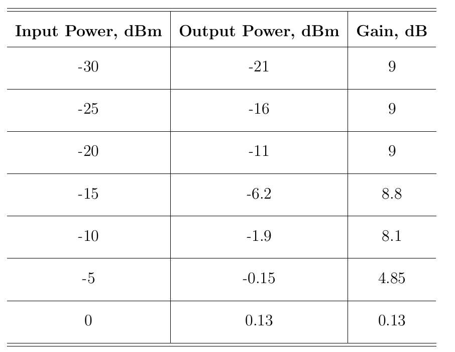
From the table above I can tell that 1 dB compression point is at around -10 dBm, again that is more than simulated -19 dBm, but smaller than -5 dBm as I expected after Network Analyzer measurements.
Investigation
Alright, after some heavy torturing of my LNA I decided to figure out the issue of DC parameters and gain/matching inconsistency with the simulation. At this point I must note something related to Layout (snapshots of which I cannot show due to the NDA nature of 7RF Kit). The Layout interconnection between Inductors and other components on chip was done on a 1.96 µm Level 2 metal. The inductor spiral was hexagonal layed at level 6 metal, another side of inductor was connected through the udnerpass Level 5 metal again to Level 2 metal for further connection to other elements.
I am now suspecting a high loss due to that layout at all frequencies. Unfortunately, at the time of Layout I could not create a better layout model for simulation as well as a 3D EM simulation. But later, I got some access to Agilent ADS Momentum package.
So, the whole idea now is to take out the inductors from my original Layout together with the interconnect lines, put them separately in a different Layout cell, export that Layout cell to Momentum view, simulate it with Agilent Momentum connected to Cadence Environment, then create the broadband model, put that model back to the original schematic in a testbench and simulate again with MMSIM.
The purpose of all this business is to achieve the same (degraded) DC and AC characteristics in a simulation which were observed during a measurements.
Inductor Parameters
I have 6 inductors in my design, three for first stage, three for second stage. Ls,Lg and Lo inductors are same for both stage. However, the interconnect is a little different, which is why I decided to make 6 different simulations with further model creation for re-simulation in MMSIM Cadence simulator.
Ls and Lo are connected in shunt configuration, Lg is connected in differential configuration in the design.
Below are the simulated resistance, Q-factor and Inductance for differential and shunt configuration of Ls inductor of first stage
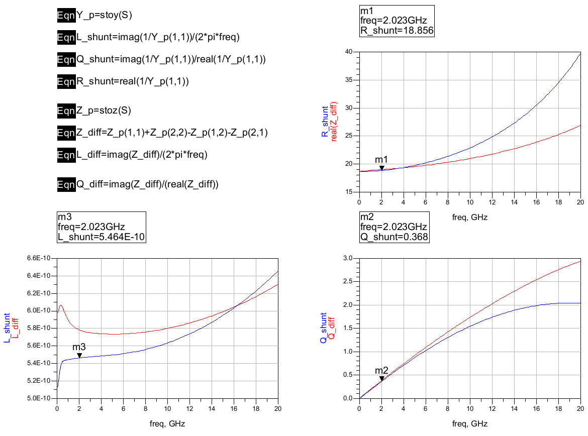
Q factor is only 0.368! That is LOW! Anyhow, moving on
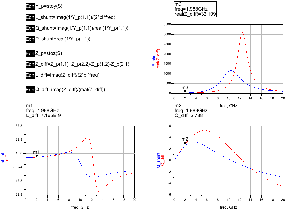
Below are the simulated resistance, Q-factor and Inductance for differential and shunt configuration of Lg inductor of first stage
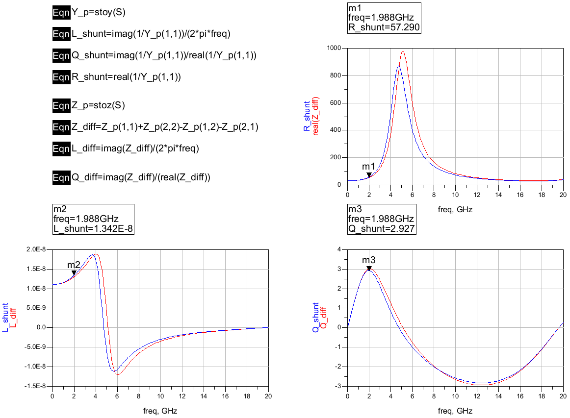
Below are the simulated resistance, Q-factor and Inductance for differential and shunt configuration of Lo inductor of first stage
Alright, now goes the second stage inductors characterization (with interconnect lines too)
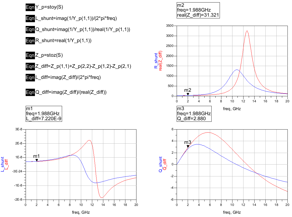
Below are the simulated resistance, Q-factor and Inductance for differential and shunt configuration of Lg inductor of second stage
Below are the simulated resistance, Q-factor and Inductance for differential and shunt configuration of Ls inductor of second stage
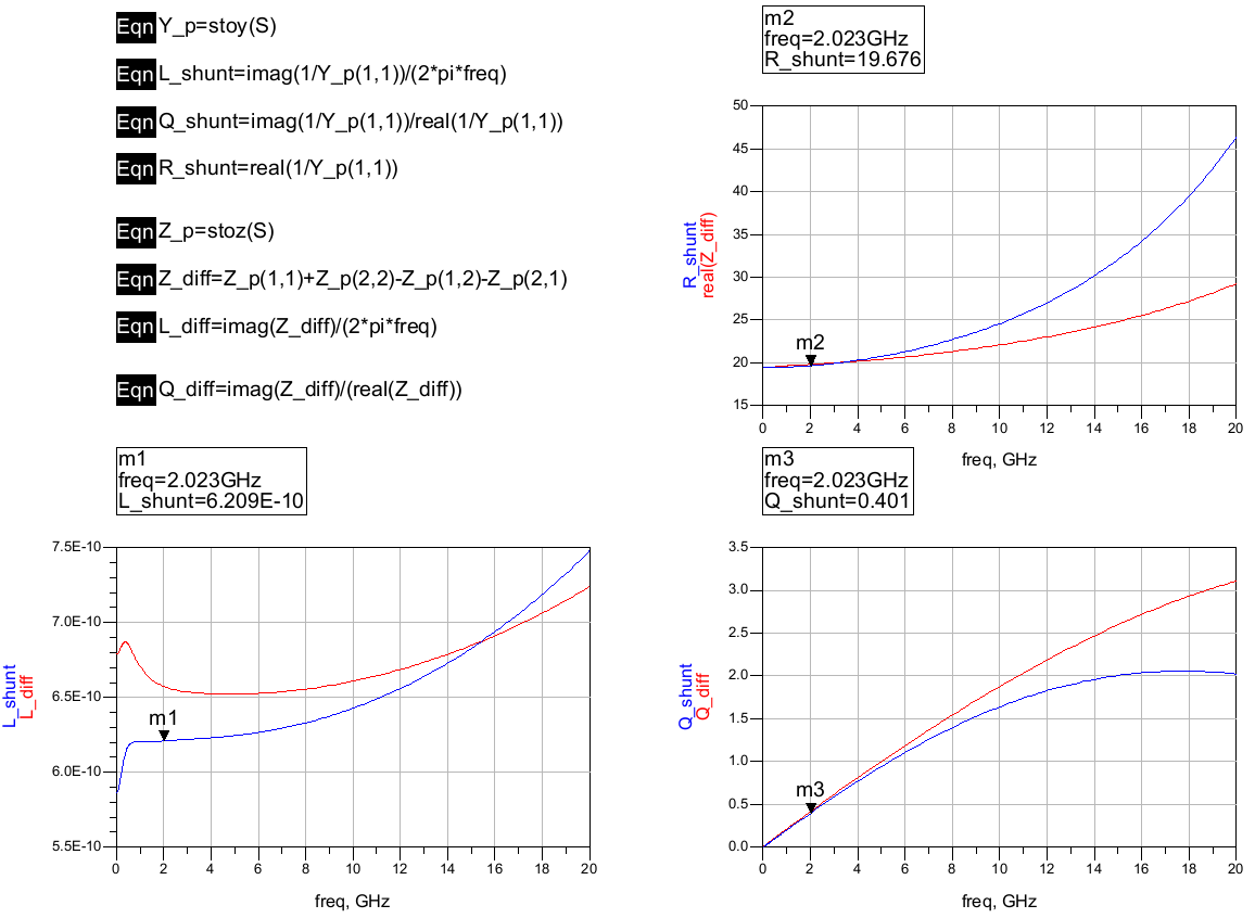
Below are the simulated resistance, Q-factor and Inductance for differential and shunt configuration of Lo inductor of second stage
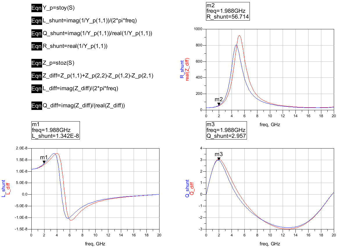
Right away I can tell that the resistance is way high at the frequency of interest for all inductors, the Q-factor for Ls inductor is terrible.
Simulation of LNA with Inductor models created by Momentum
The broadband inductor models were created from Momentum after the simulation. I put those models in the modified schematics of my LNA as shown below
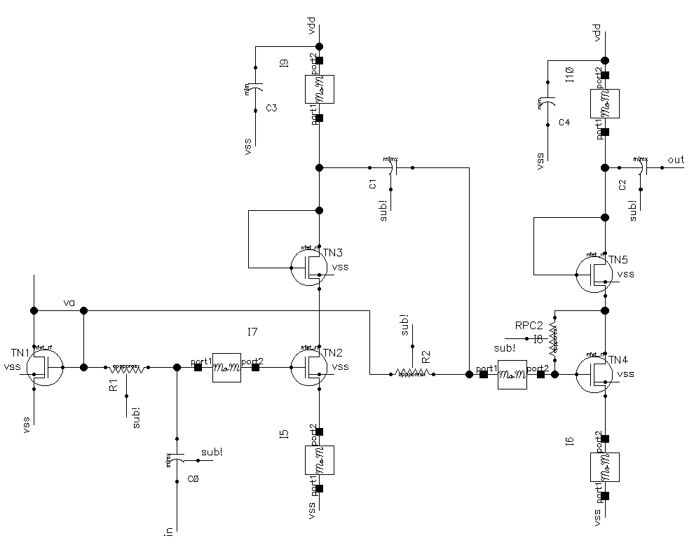
After that I first reran the DC simulation. As a result, I see completely different DC characteristics than from previous simulation, and now those DC characteristics are closer to what I measured! Below is a table with simulated results with Momentum models for inductors shown in the third column
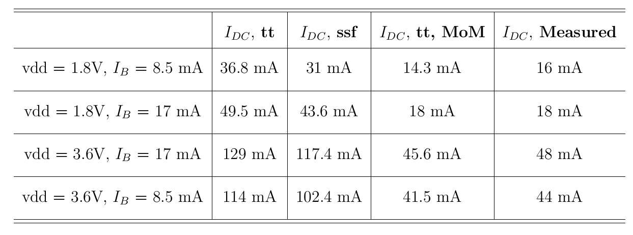
The last column shows the measured results which I showed before, where I mentioned that DC current measured at supply line looks much smaller than simulated, which can now easily be seen in this table if you compare it to the first column results (normal corner) and second corner results (slow corner). However, the results of third column (simulation under normal corner but with Momentum models for inductors) and results of last corner (measured results) are almost matched!
Now from all the information above, it turns out that inductor interconnect had a huge impact which I couldnt see before. And that impact can be even observed right here at DC.
After I simulated the S21, it turned out that at frequency of 2 GHz it was only 7 dB! Now, that is much closer to measured 9 dB gain than simulated 23 dB during the design using the standard inductor models from Design Kit integrated into Spectre.
I want to stress here that the problem is not that much in a Spectre models of inductors from Design Kit, but rather the way how I layed out the interconnect. The Momentum models of inductors were simulated including the interconnect lines from inductor ports.
Alright, after all that I want to re-design the LNA, but this time rely heavily on the Momentum simulation. I decided also to simplify the LNA from the schematics point of view, I do not want to have now two stages, just one stage, and no resistive feedback, also I will implement the blocking capacitors off-chip, this will give me more freedom for measuring the DC parameters. The redesign is covered here!

