
2 GHz Simplified Common-Source Low Noise Amplifier
This is a remake of another LNA. The purpose of the remake is to design a simpler common-source amplifier with on-chip inductors and their interconnects modeled in Agilent Momentum package, successfully test it and observe a better correlation between simulated results and measurement results.
Design
The design consists of just a biasing transistor, main amplifying transistor and diode-connected transistor. Layout is shown below

And the schematics is shown below.

Another change which I decided to do is to increase value of RPC0 resistor to 10 kOhm, in a previous design it was 2 kOhm. Higher resistance will provide a better input RF signal block from the bias line.
Inductors Simulation
The next thing I did was a preliminary simulation. After that I did the layout. Then, I took the layout of inductors from the design layout together with a new interconnect lines which now were 10 µm wide and realized on level 6 and level 5 metals and put them to a separate Momentum cell for simulation.
So below goes the simulation of Lg inductor

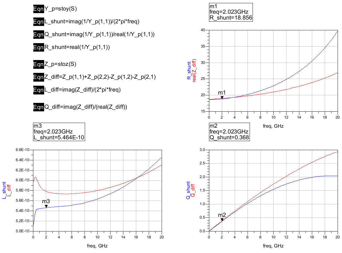
Below goes the simulation of Ls inductor

Below goes the simulation of Lo inductor

The first thing I notice right away is 2 Ohm resistance for Ls inductor at 2 GHz compared to 18 Ohm resistance for the Ls inductor of previous design! Also, the Q-factor is now 2 instead of around 0.4.
Simulation
Now after the inductors have been simulated and their models were created, I reran the Cadence MMSIM (Spectre) simulation with those Momentum models for inductors and their interconnects.
I also modified the testbench, since there are no on-chip blocking capacitors at the input and output, the capacitors will be off-chip. So I included the S-parameters model of those C0G class capacitors from Kemet. Modified testbench schematics is below

S-Parameters Simulation
Below are S-parameters simulation plots


You can see now 13.6 dB gain and -18.9 dB S11 parameter at frequency of 2 GHz. Again, that is given the fact that Momentum generated Inductor models with their interconnects were used in a simulation. Below is a Noise Figure simulation and it can be seen to be around 3.1 dB

Here is one more thing I did, I removed the Momentum models, and put in the Spectre models for the given inductors. This way, I removed the effect of the new interconnect and inductor models provided by Momentum, then I imulated S21 and S11 again, below is a result

Now, it turns out that the Spectre models combined with absence of interconnect modeling gives different result, but again, result is not too much different, the S11 is now around -15.6 dB instead of -18.9 dB and gain is now 16.1 dB instead of 13.6 dB as in previous simulation.
This again proves that interconnect of inductors has huge impact on results, but it has less impact when done more properly. So even at frequencies around 2 Ghz which is not considered super high, it is better to take into account the physical layout interconnect during a simulation, and preferably do it with a proper tool.
The design was submitted to another MOSIS run for 7RF 180nm IBM process. Once the chip comes from fab, I will do the same tests, however; I will perform another set of tests as well with another set of measurement equipment. Then, I will add corresponding simulations sections too. I hate waiting for chips, it takes couple months or so to get them back. I wish that waiting period was 1 week ;]