2 GHz Common-Source Low Noise Amplifier
Here I will be showing a common-source LNA design with a target frequency of 2 GHz for IBM 180nm 7RF process. I will cover the design, simulation and experimental results.
Design
Before showing off the schematic I will just present a basic model of LNA in a common-source MOSFET configuration together with its analysis. The schematic of this model is shown below
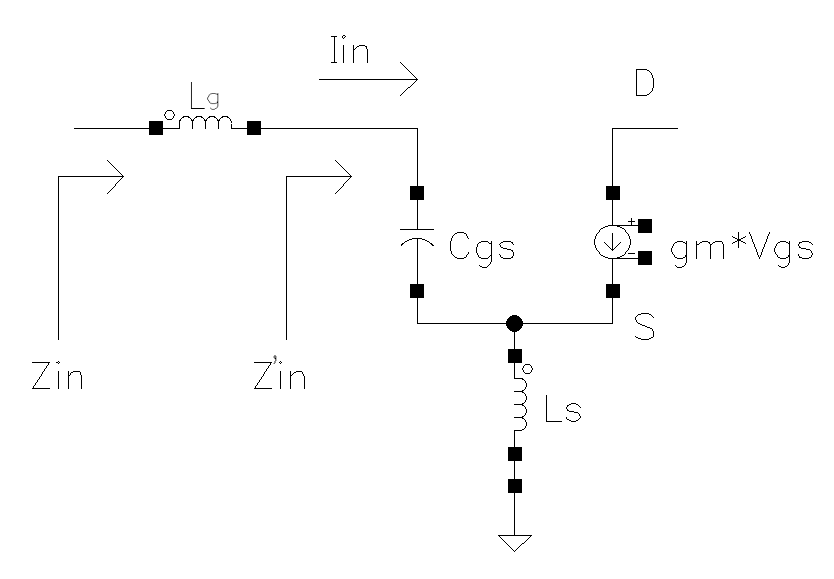
The analysis of the model starts with the nodal equation for a node S

After that I can work my way deriving out Vg - Vs
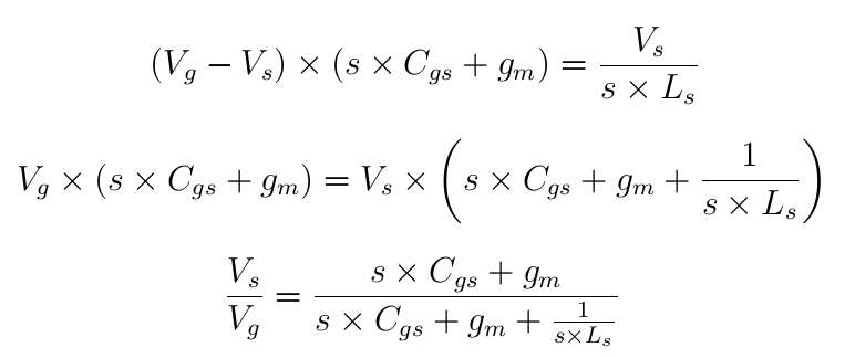

Now I am deriving the current Iin


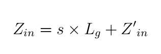
The impedance looking into the gate is

where second term represents the real part. The natural frequency at which I want my amplifier to be tuned is

Where L is the total inductance and equals Lg + Ls. The transition frequency is defined as

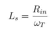
Now I can write Ls as
The impedance looking into Lg is
Now I can start picking up a values for the components, keeping in mind that the amount of inductance I can use on chip is limited. I decided not to exceed 8 nH inductance for Lg + Ls. So, I am using 8 nH for L. Now, from the formula of natural frequency with Cgs I can write
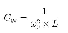
Using 8 nH for L and 2 GHz for f0 I get 791 fF for Cgs. Based on the calculated value of Cgs, I can write

Using the values of 0.745 fF/µm and 8.42 fF/µm2 for Cgso and Cox, 0.18 µm for Length of transistor and calculated Cgs of 791 fF I get 450 µm for the width of transistor W. Of course the values which I used to calculate W are very rough approximates for typical 0.18 µm process. That is why I just decided to further tweak all values after initial simulation.
The next stage is to calculate gm

using the values related to 0.18 µm process and Vgs - Vth of 0.15V it turns out to be 117 mA/V. Knowing gm I can calculate current

which turns out to be 8.8 mA
Now assuming ideal input impedance of 50 Ohm and using the value of transition frequency I calculate Ls inductor to be 338 pH. Subtracting it from total L of 8nH I get 7.66 nH for the gate inductor Lg.
Finally I can construct the schematic. The schematic is shown below
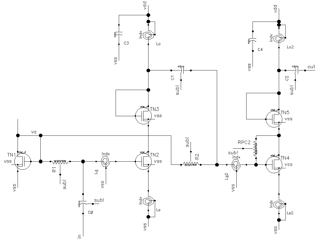
The TN1 is a bias transistor, TN2 is the main amplifying transistor for which the model above was analyzed, TN3 is the diode-connected transistor, C0 is the blocking capacitor, C3 is the decoupling capacitor, Lo is an RF choke and R1 is a signal blocker at the biasing line. The second stage has similar components, except the RPC2 feedback resistor for the output matching improvement, its effect will be discussed later.
Of course the design will need a heavy tweaking, first of all input impedance not going to be 50 Ohm, it is affected by many factors including the package parasitics, pad parasitics, ESD cell parasitics and other parasitics present at the RF input line such as interconnect parasitics from the DC bias line. So I am going to put the initial design in the testbench with approximate values of all other elements which will be present in the final LNA. Schematics of that testbench is below

After running couple simulations, I tweaked the width W of the main amplifying transistor to be 277.2 µm, as you see it is much different than initially calculated value of 450 µm. Similarly, I made all other transistors except biasing transistor to have 450 µm width as well. The biasing transistor is twice less in width.
Simulation
Here I will be showing the simulation results.
S-Parameters Simulation
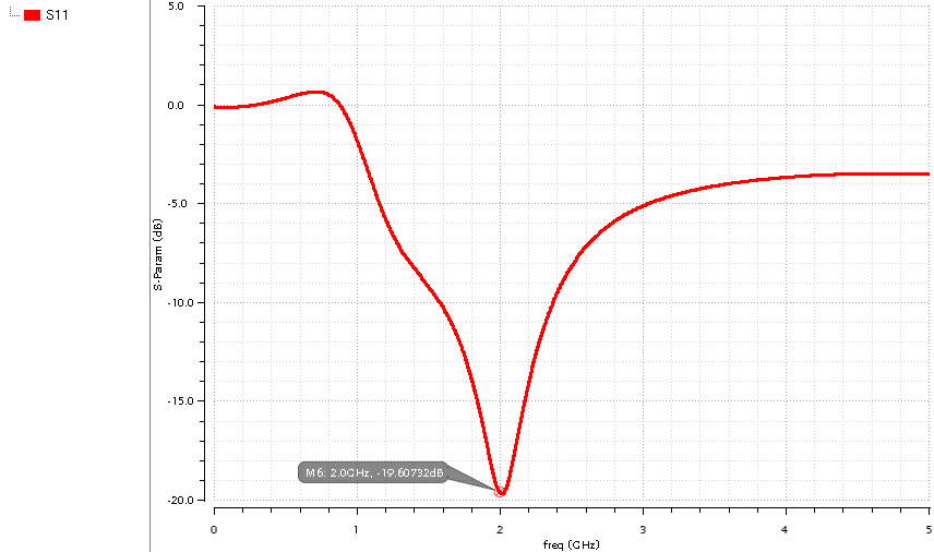
S11
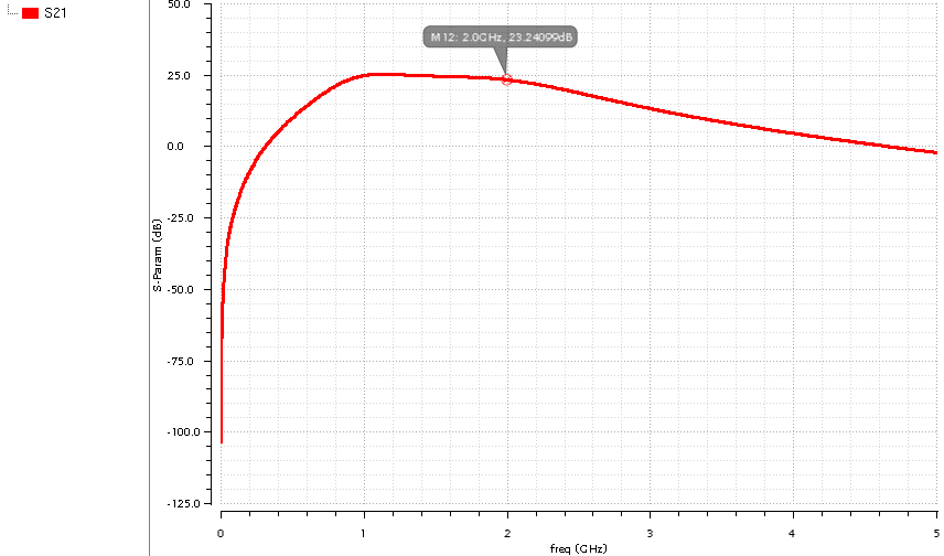
S21
S22
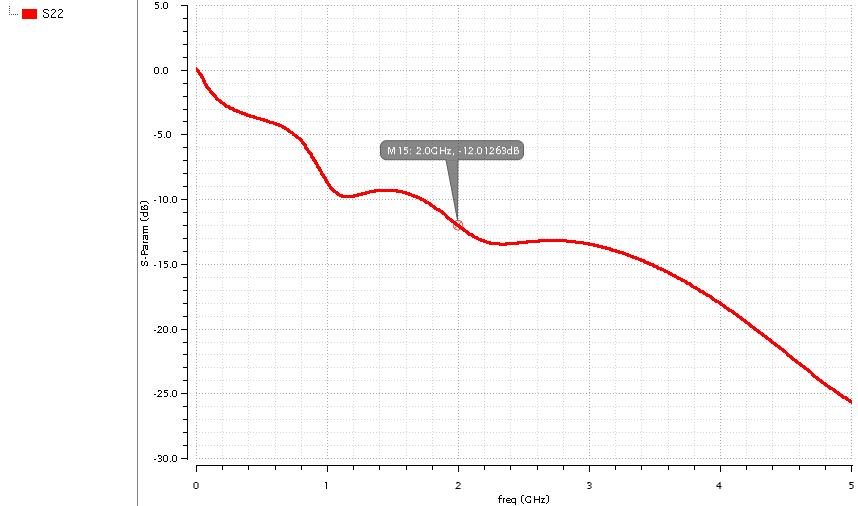
S12
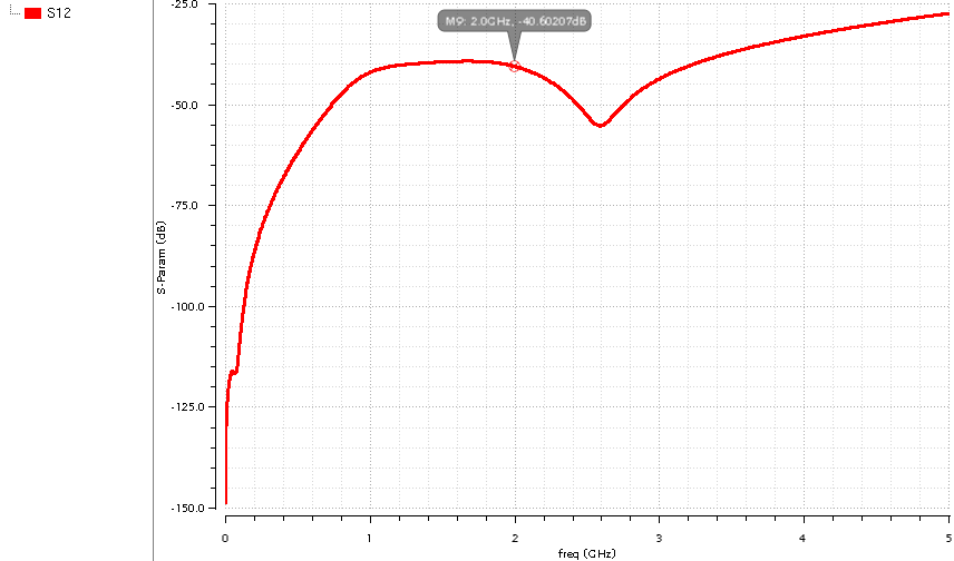
The feedback resistor at the second stage as I mentioned before, improves the output matching, but at the price of a little reduced S21 gain. Below is a simulation of S22 parameters without that resistor
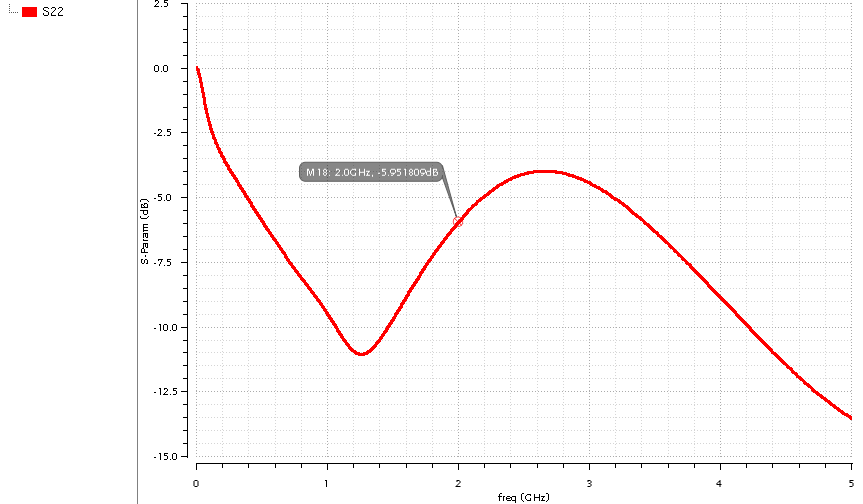
As you see S22 at the frequency of interest is now -5.95 dB instead of -12 dB as in a previous plot. Of course in case if the amplifier is supposed to be a standalone module to be used with a systems with 50 Ohm impedance then we want smaller value of S22, i.e. better output matching to 50 Ohm, but if the LNA is to be used with some another block on-chip whos input impedance is not necesseraly 50 Ohms then amplifiers output impedance has to be matched to another value.
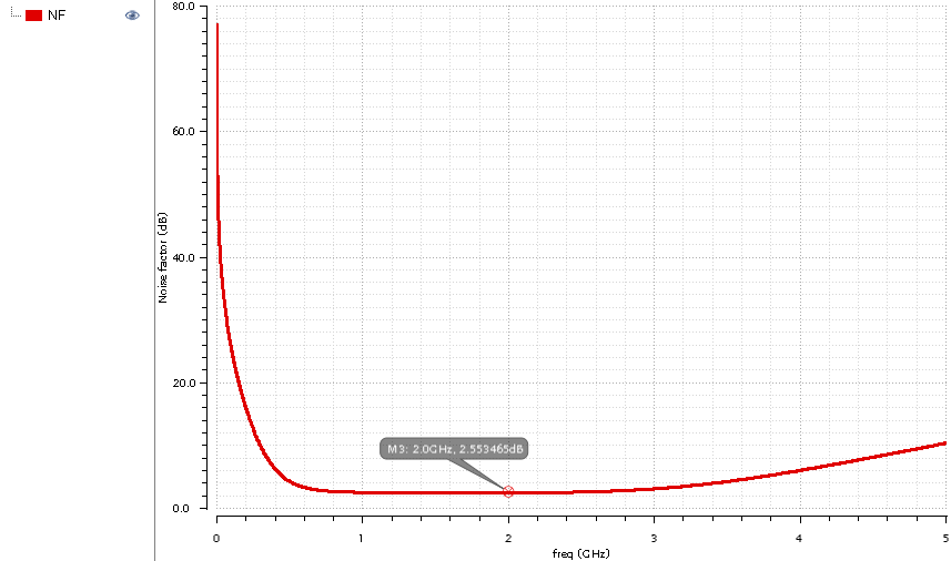
The Noise Figure simulation plot is shown below. At the target frequency Noise Figure is 2.55 dB.
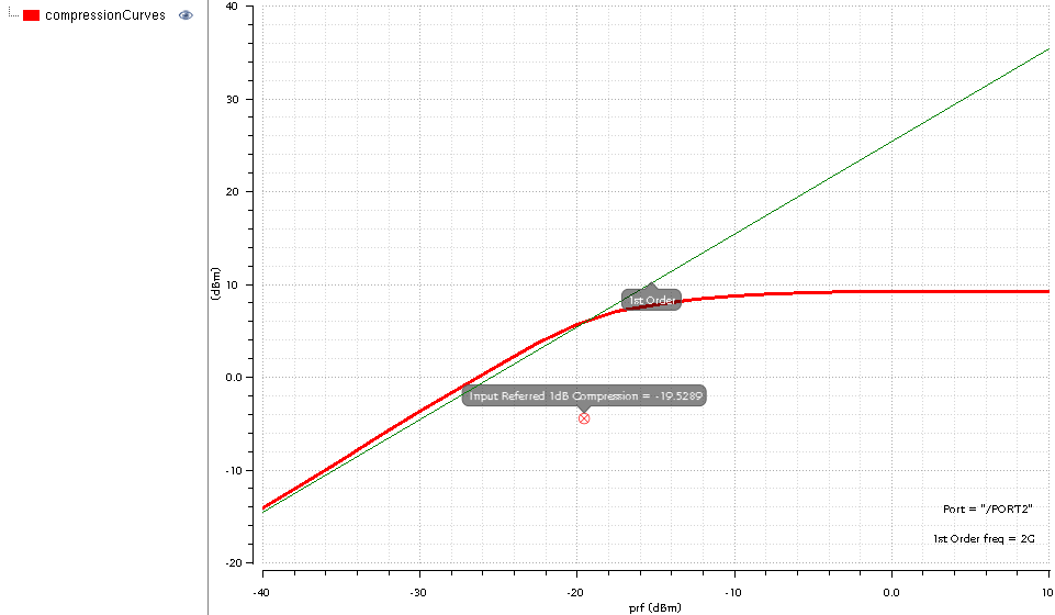
Input referred 1 dB compression point simulation is shown below and it is -19.5 dBm.
The layout was done and integrated into the custom designed pad frame whos elements were parts of the simulation testbench of LNA. The whole design was submitted to MOSIS run for IBM 180nm 7RF process.
Test PCB
The schematics of test PCB is shown below
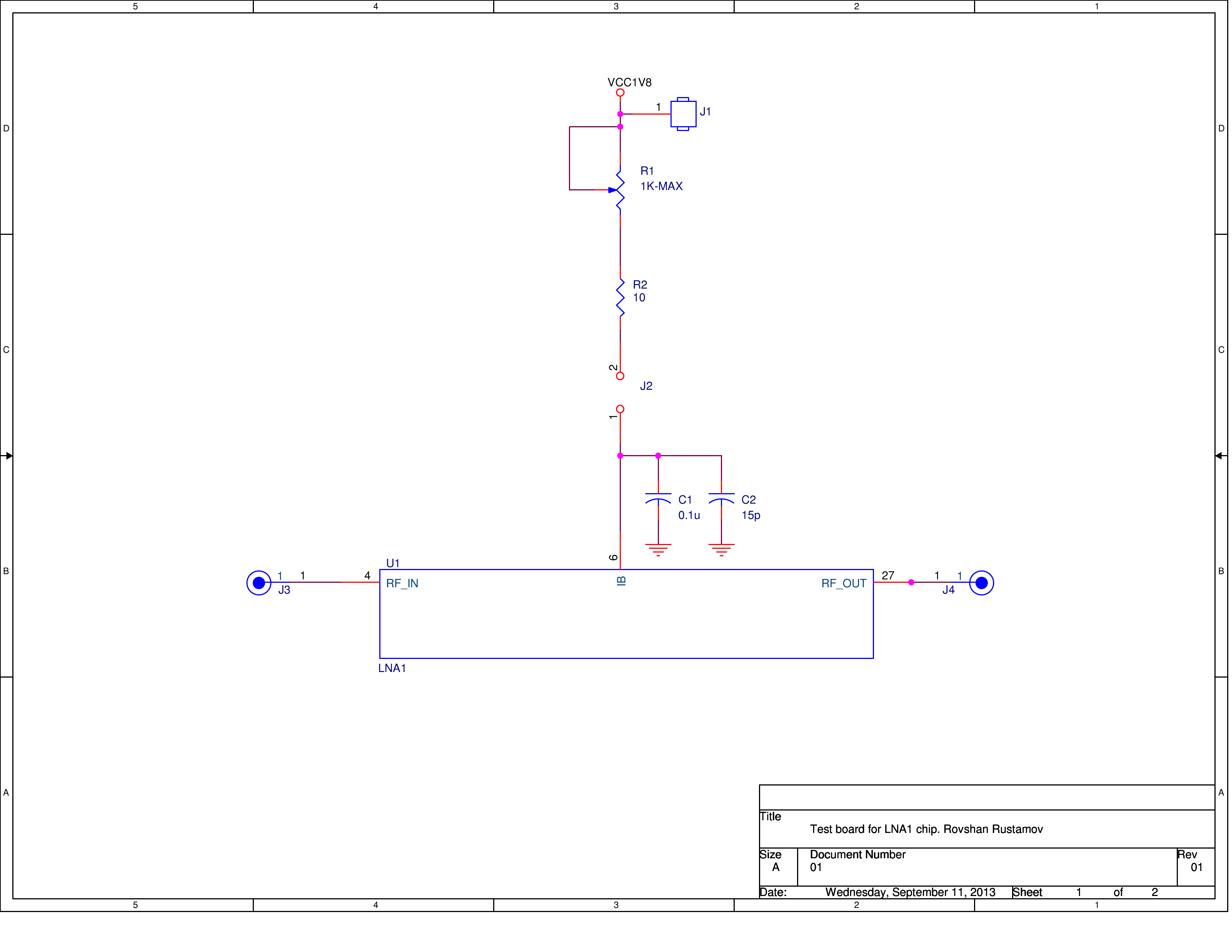
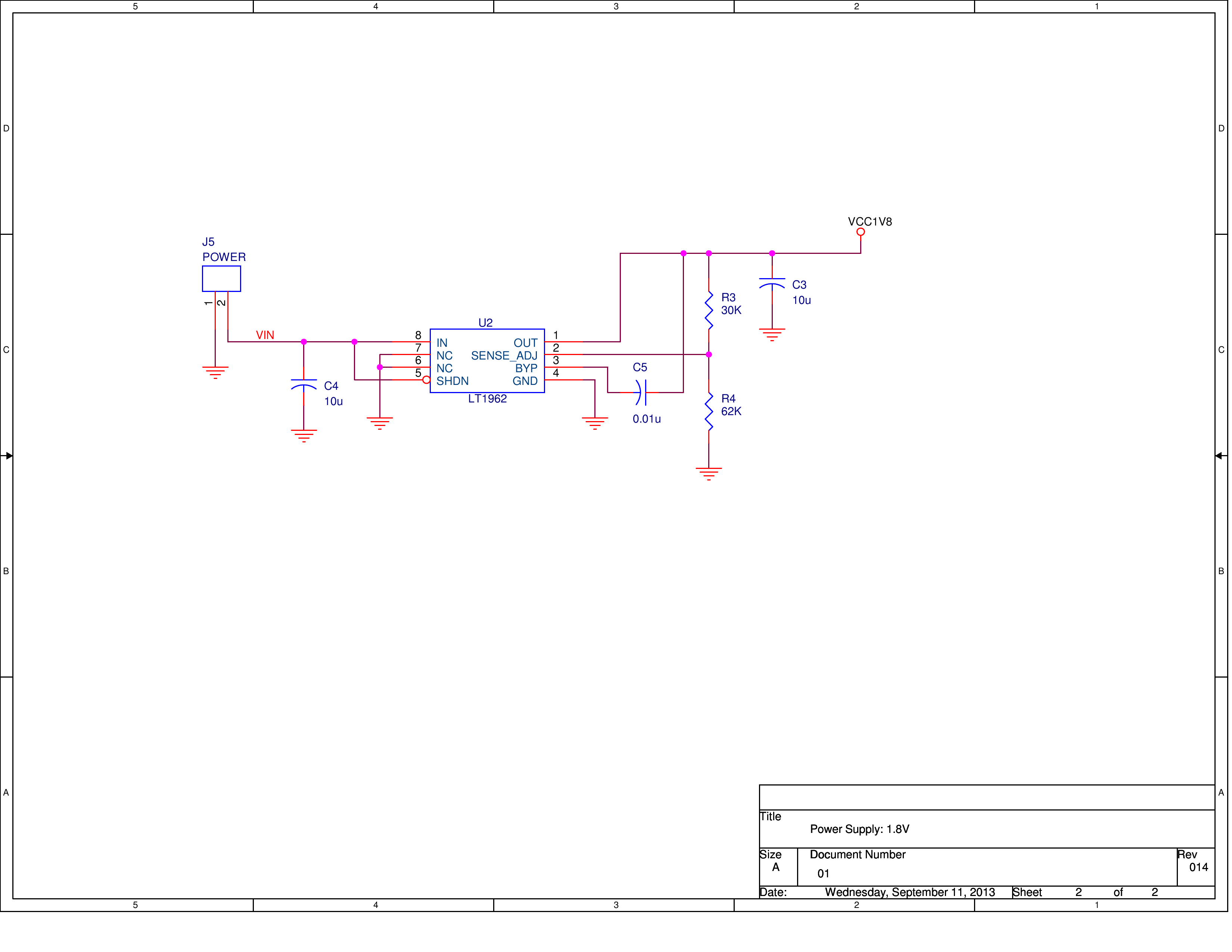
The R1 is a variable high quality 25-turn Bourns resistor for biasing, R2 is maximum current set resistor, C1 and C2 are decoupling capacitors. PCB will also include an on-board LDO from Linear Technology.The PCB was made on the process described here.
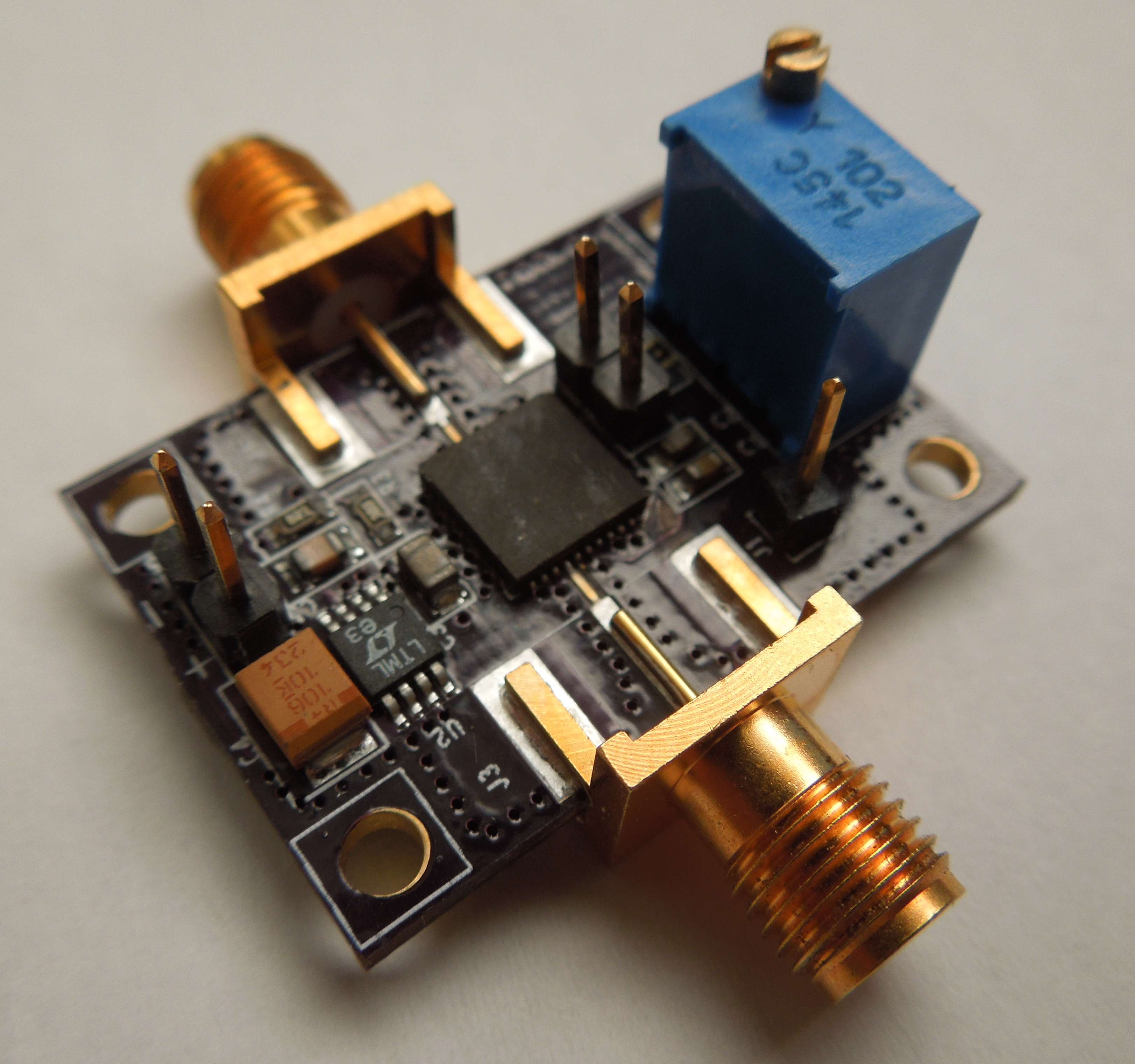
Below is a photo of assembled test PCB with the LNA chip received from MOSIS in a QFN40 package (typical package I use for most of my test custom ASICs).
Now it is testing Time!

