Digital Test Chip for IBM 180nm 7RF Process
Experimental Results
Measuring the Ring Oscillators
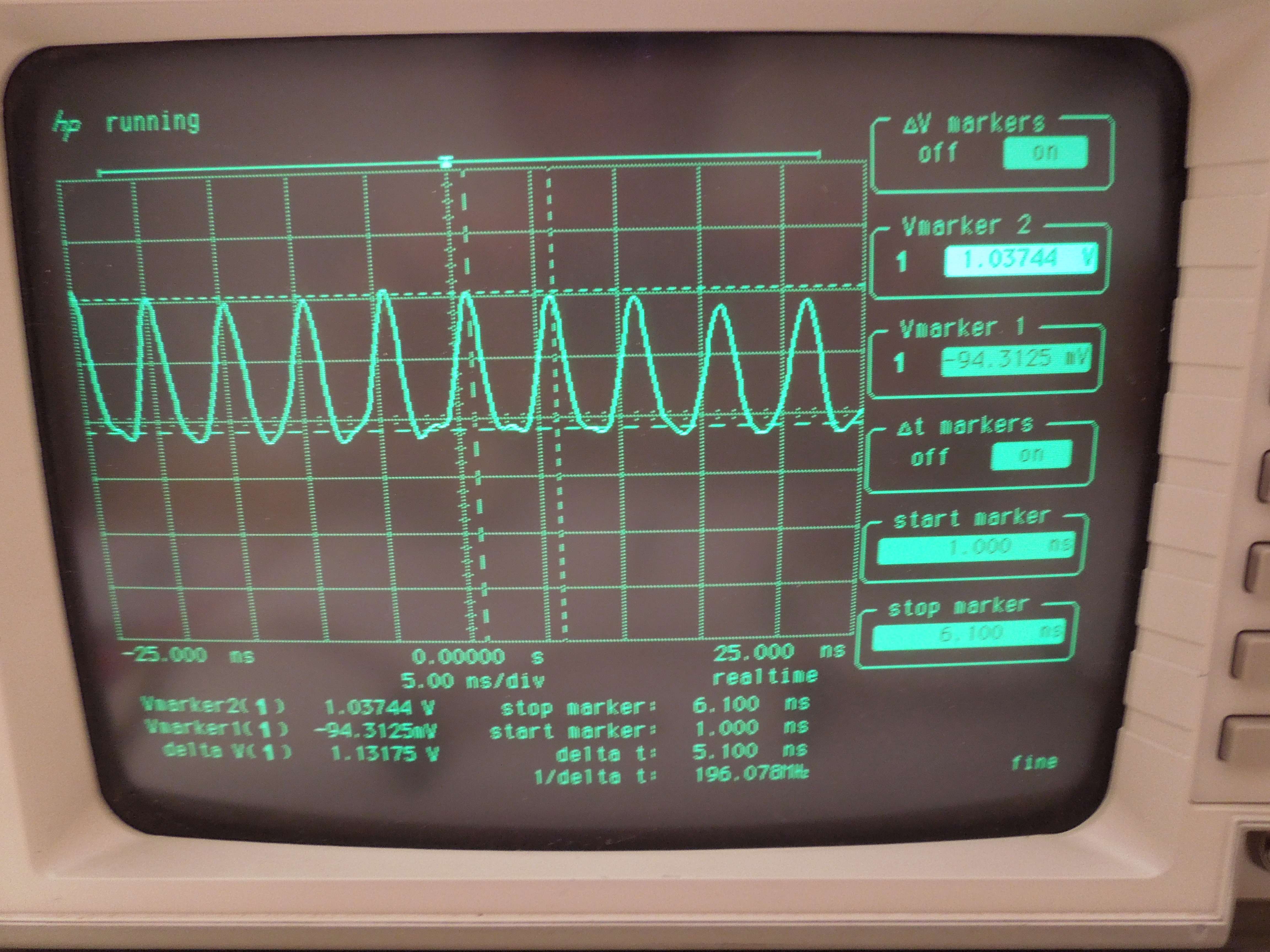
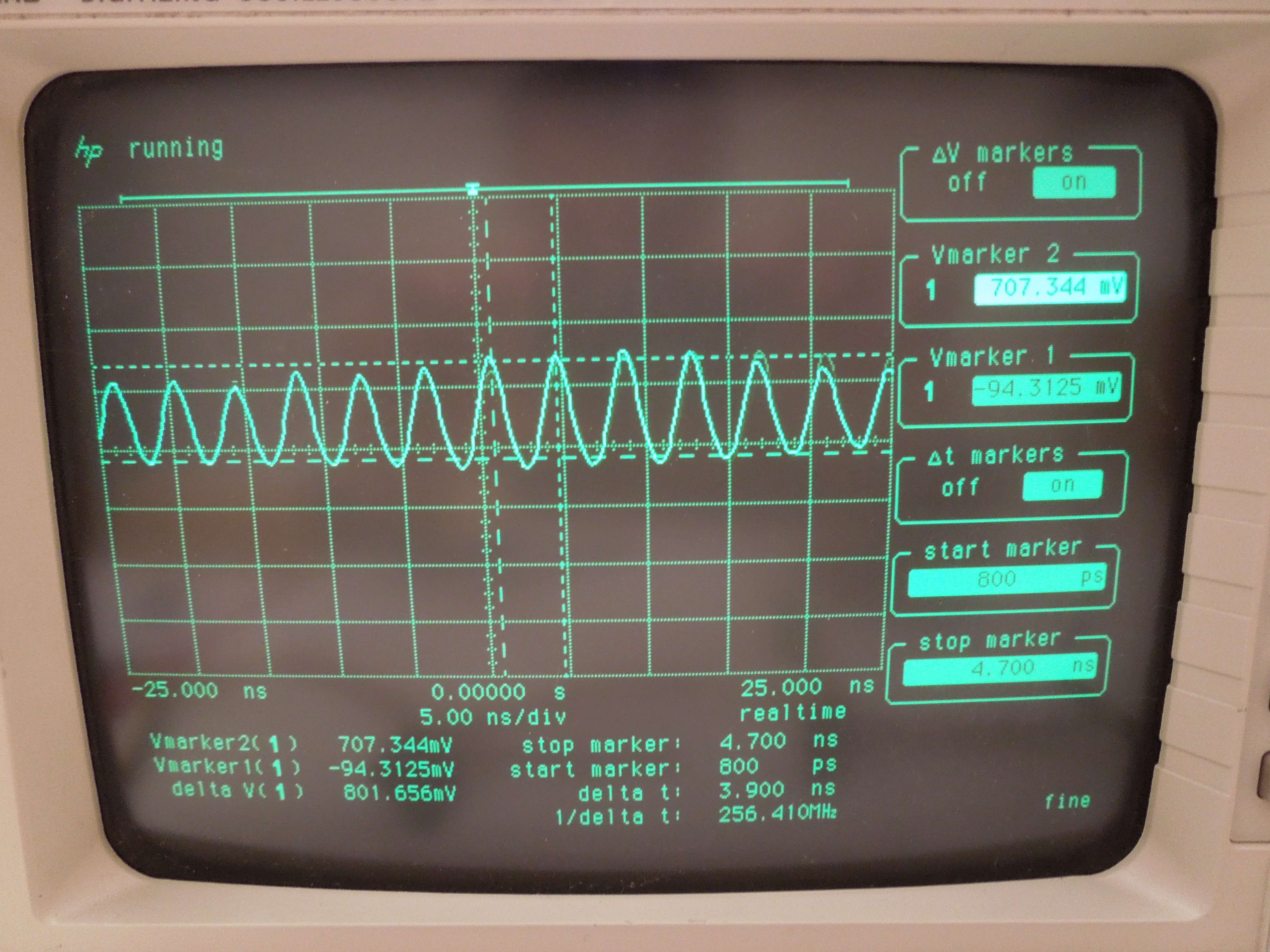
First, I powered up the board, then I turned on power for one of the variable supply ring oscillators. I took 24 measurements starting at the supply voltage of 0.69V and going up to 1.15V with increments of 200mV. Below are snapshots of four of those measurements
Measurement with 0.69V supply
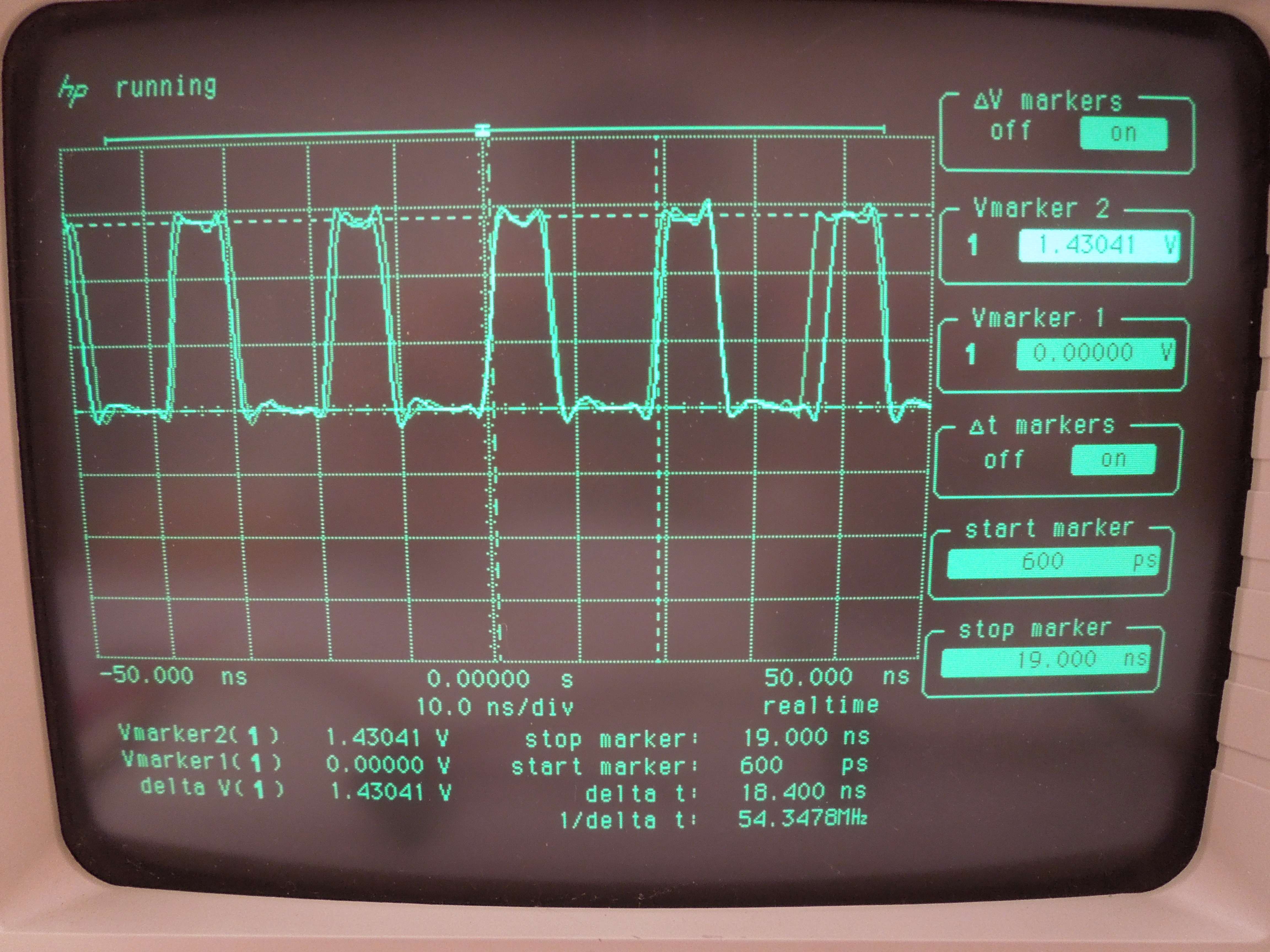
Measurement with 0.79V supply
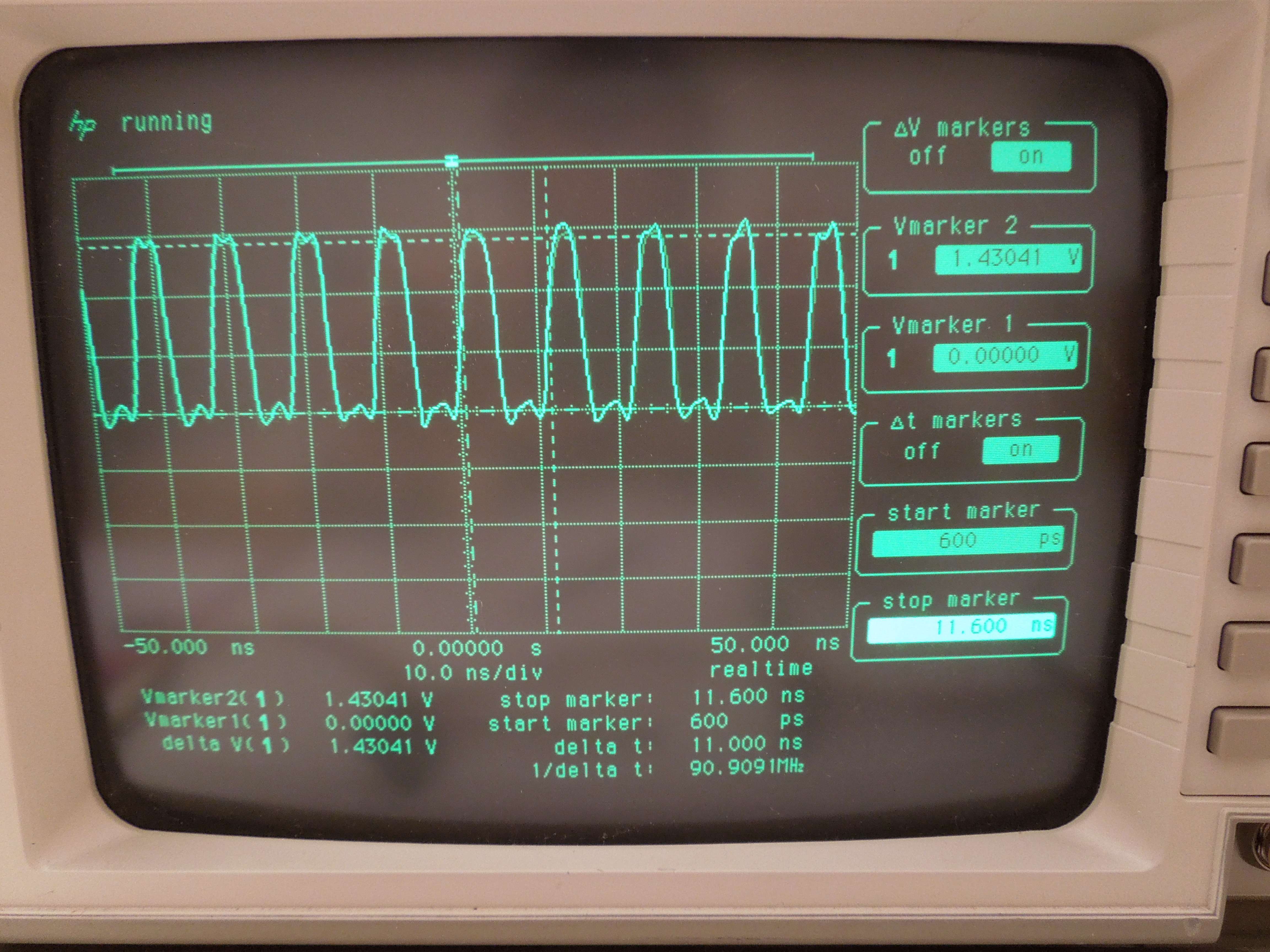
Measurement with 1.03V supply
Measurement with 1.15V supply
Below is a picture showing the plot again with simulation results, as well as the measured frequency results of the variable supply ring oscillator which varied only up to 1.15V.
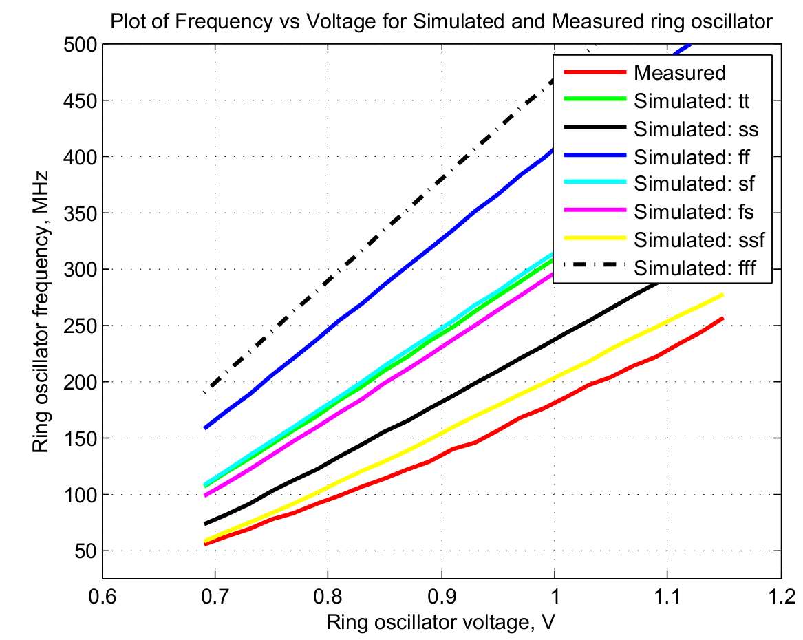
The first thing we can notice right away is the fact that the ring oscillator turned out to be slower than the slowest corner simulation! You can see the yellow and red traces on the plot. They are not terribly far apart, but they are noticeably apart.
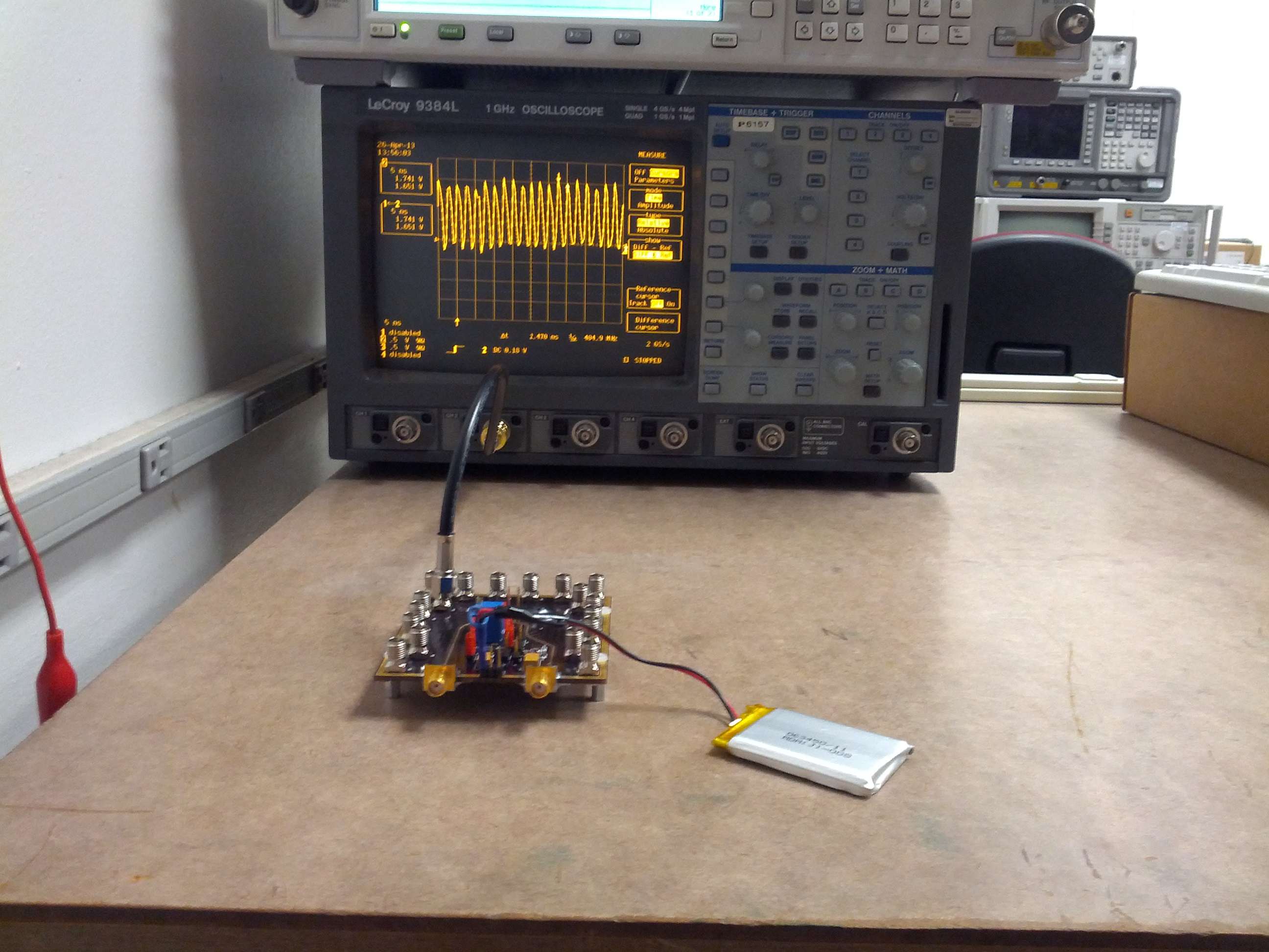
Next, once I got my hands on a better scope, specifically LecRoy 9384L, I measured the output from the ring oscillator with a fixed 1.8V voltage supply. And plots are shown below. The big picture of setup
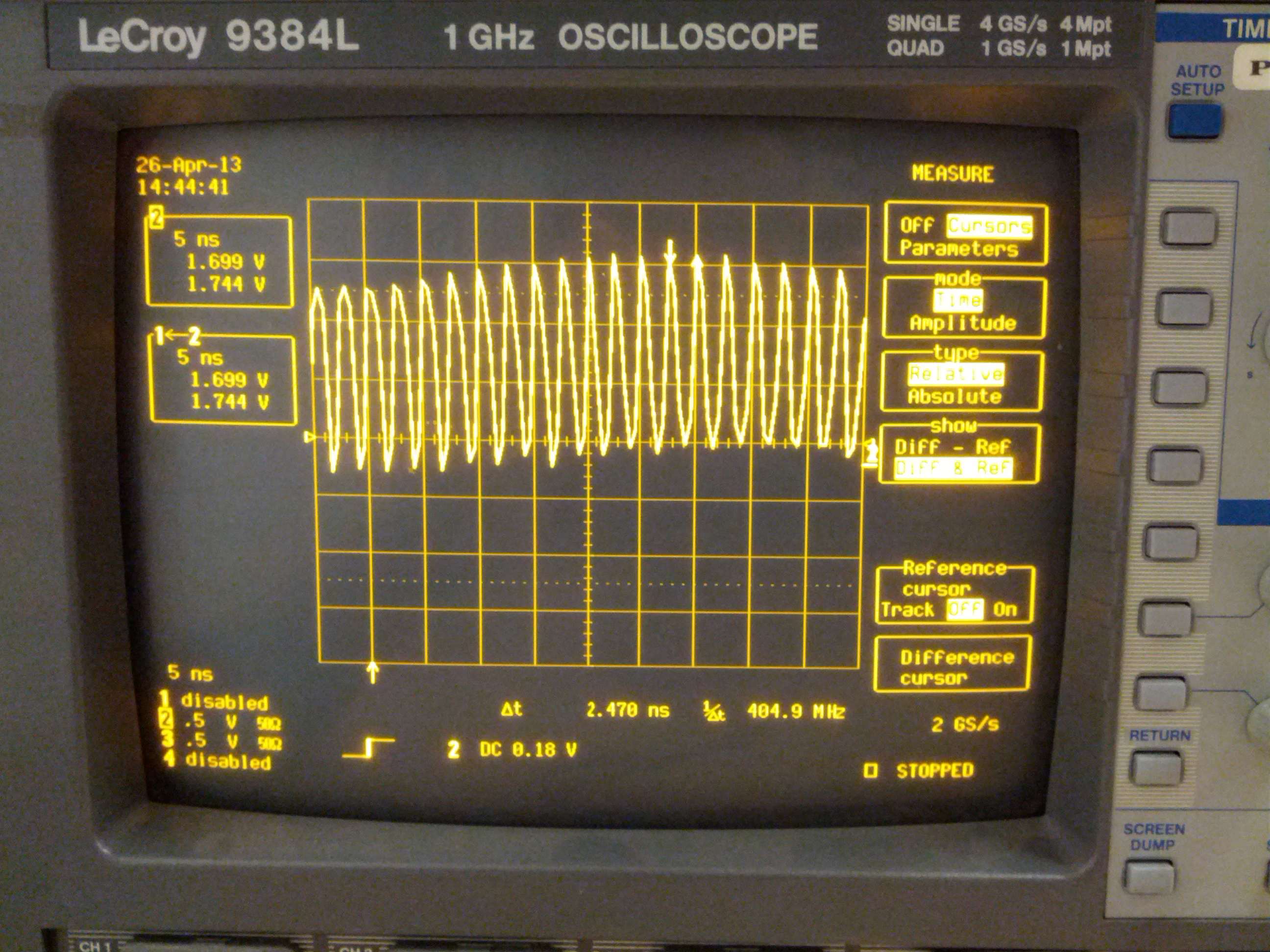
Frequency measurement
Amplitude measurement
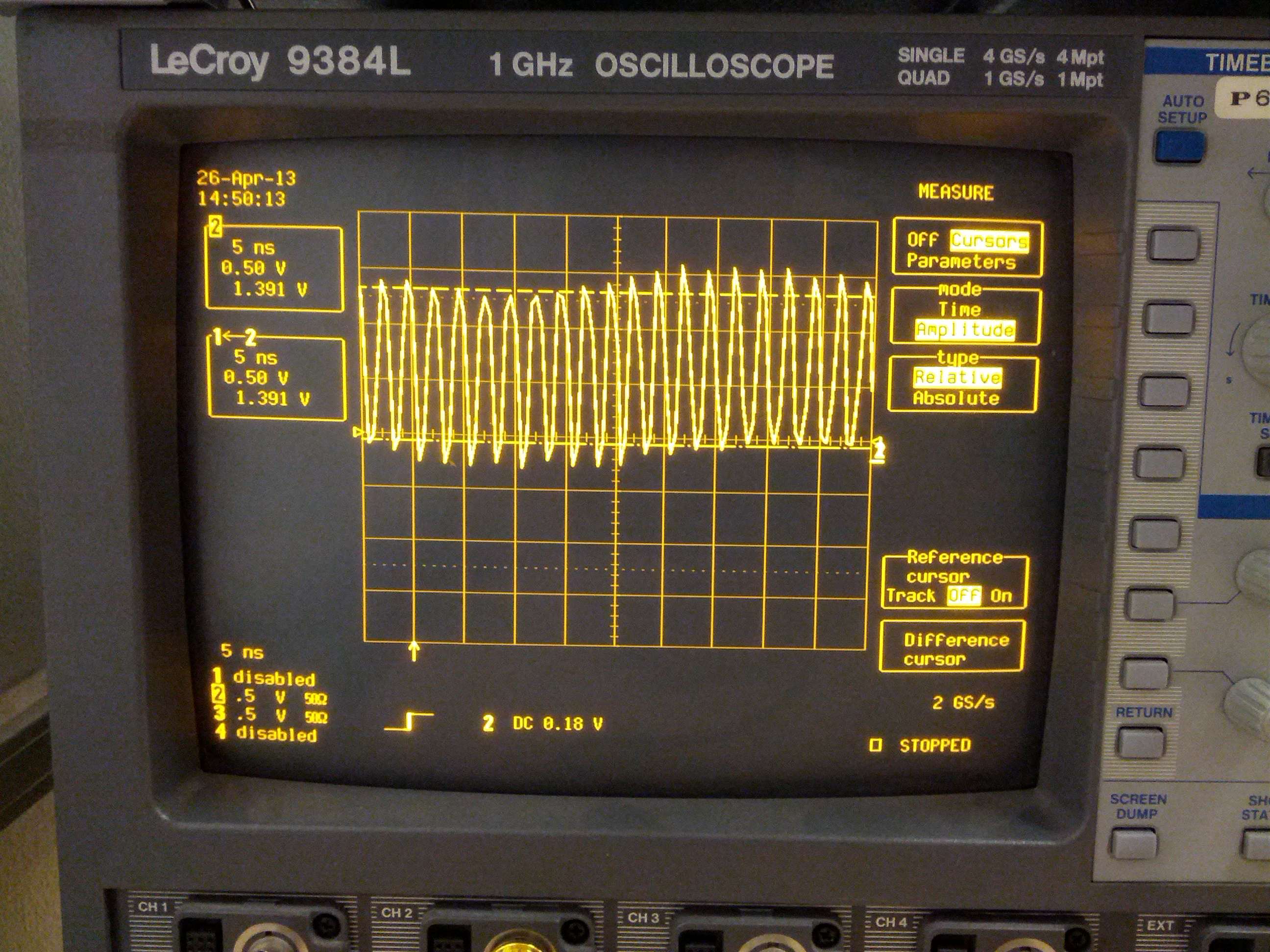
So, the frequency is 404.9 MHz and the peak-to-peak amplitude was measured to be around 1.344V. Recall, that in a simulation we got a frequency of around 750 MHz simulating this Ring Oscillator with 31 stages and 1.8V supply voltage. So, this turned out to be pretty far from the normal corner.
After that, I also checked the frequency of the signal using a E4403B Spectrum Analyzer. (of course, care has to be taken in order to not exceed the allowed power level at the input port of Spectrum Analyzer). Below is a plot
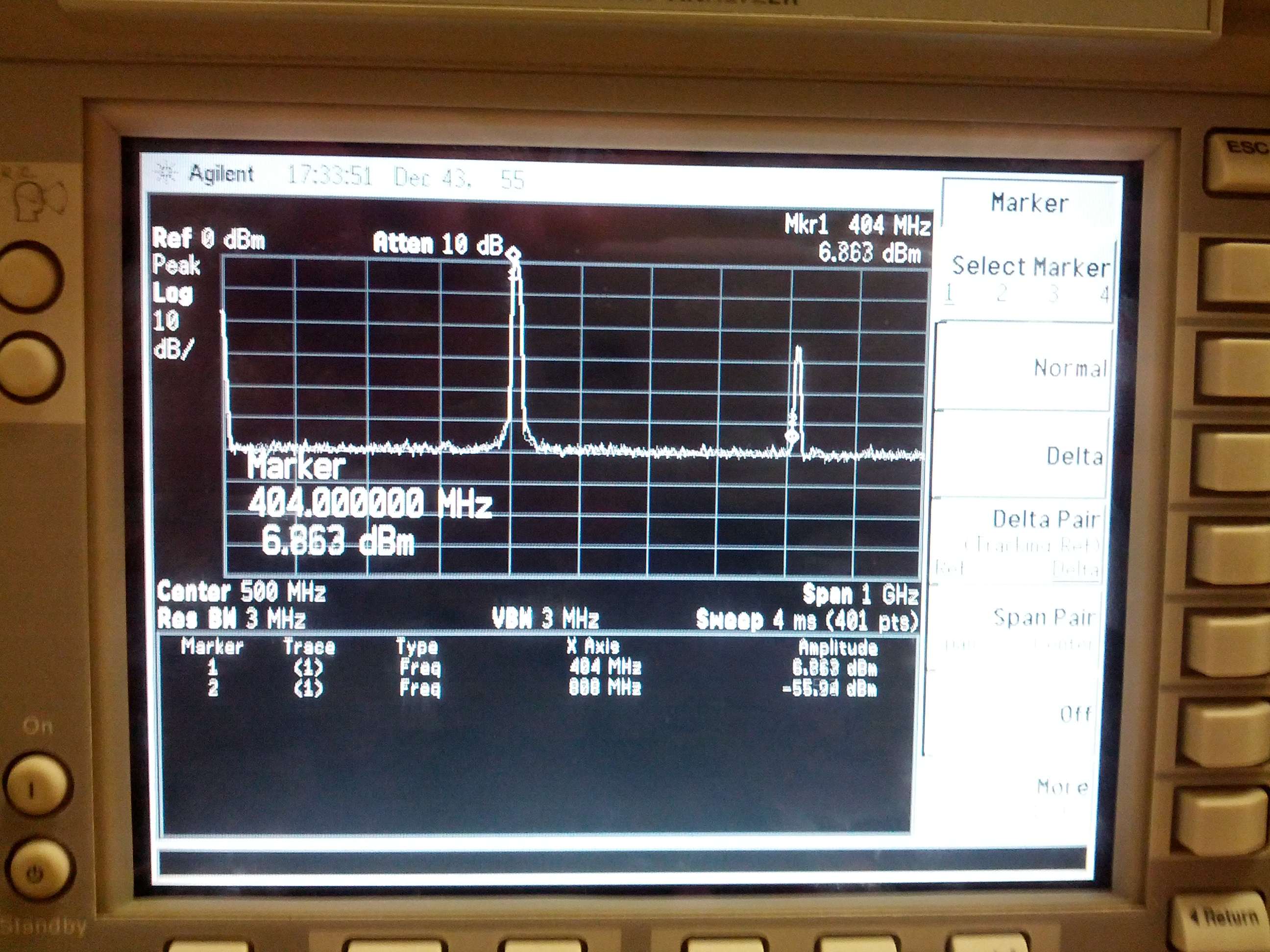
We can see around 6.8dBm at 404 MHz, the signal is not right at that frequency though, the second harmonic does not have a peak right at 808 MHz.
So, we can conclude that Ring Oscillator and the voltage level converter work, it just turned out to be a bit slower than the slowest simulation corner. Another thing worth to mention is that variable supply ring oscillator with voltage level converter worked starting from about 0.69V, which is why that voltage was selected as a starting voltage.
Measuring the Digital Buffer Performance
Now it's time to mess around with a Digital Buffer. I have placed some Digital Buffers on a chip with input tied to one pad and output to another pad. This will allow me to pump high-frequency signal into the buffer and continue increasing frequency until I won't see signal at the output of the buffer with reasonable power level. I used the signal generator to provide signal to the input of the buffer. The test PCB also had an addon with sinusoidal DC offset shifter, so that negative amplitude of sinusoid from signal generator wont appear at the chip inpud pads.
Below is a measured Digital Buffer output signal when the input signal is 500 MHz
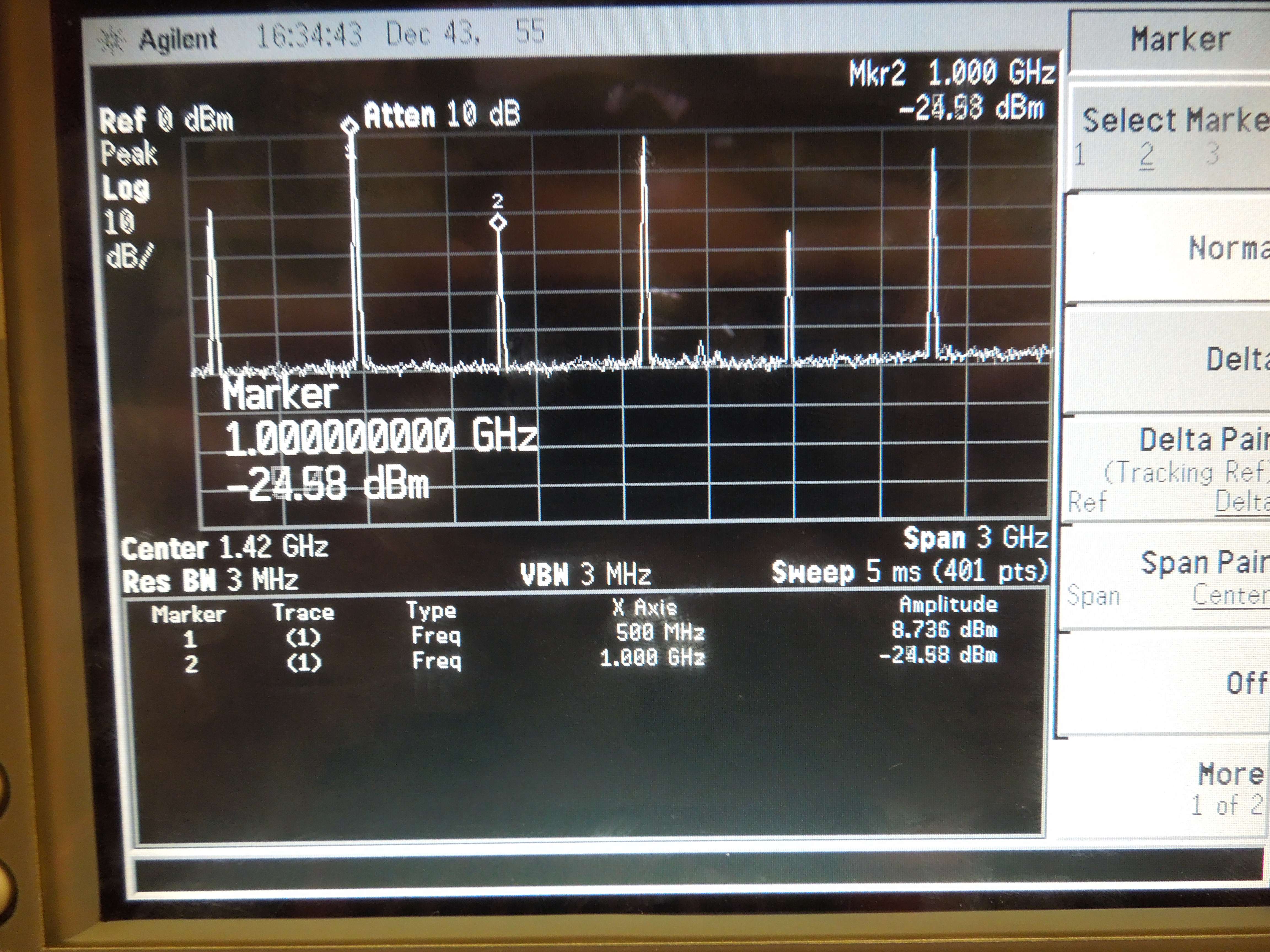
Below is a measured Digital Buffer output signal when the input signal is 1 GHz
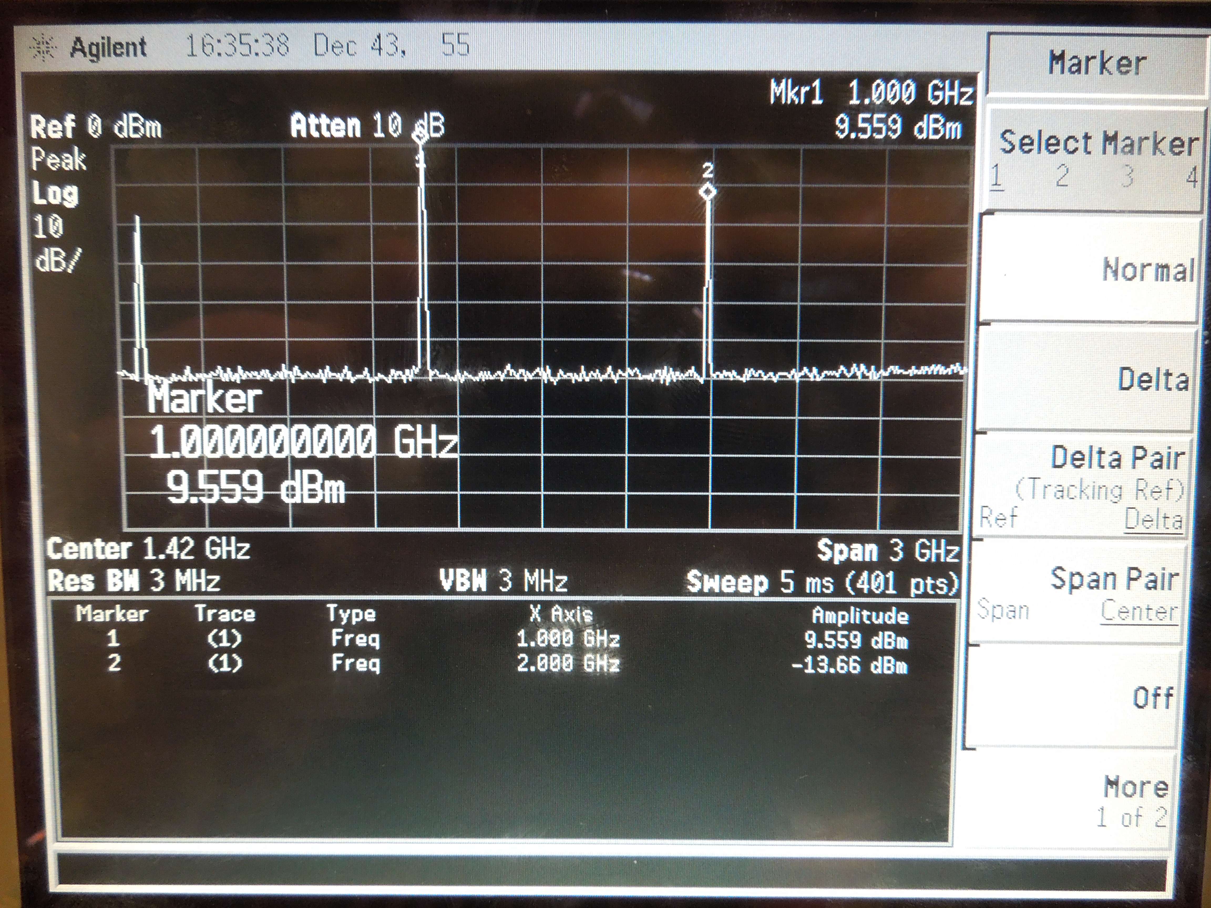
Below is a measured Digital Buffer output signal when the input signal is 1.5 GHz
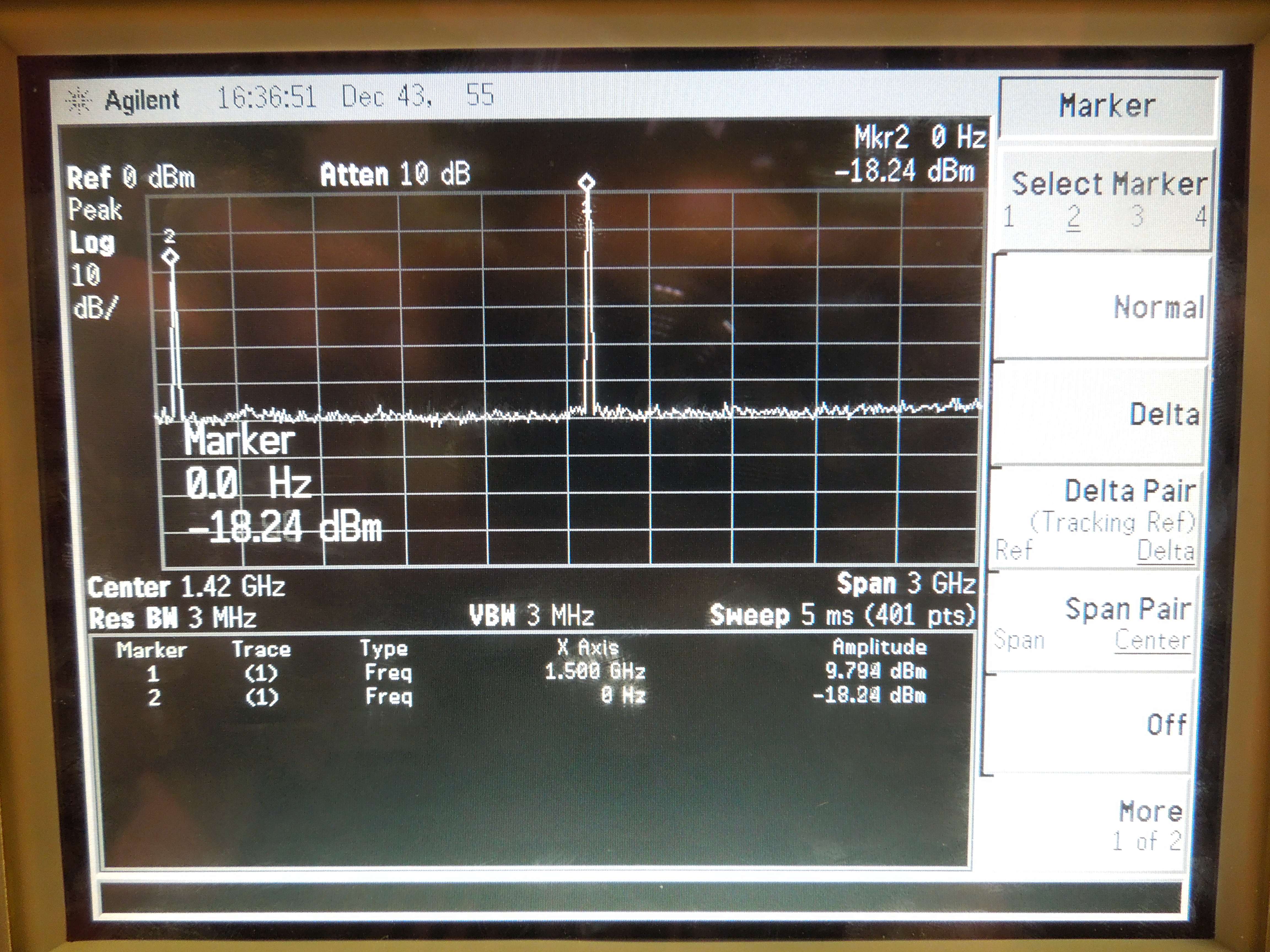
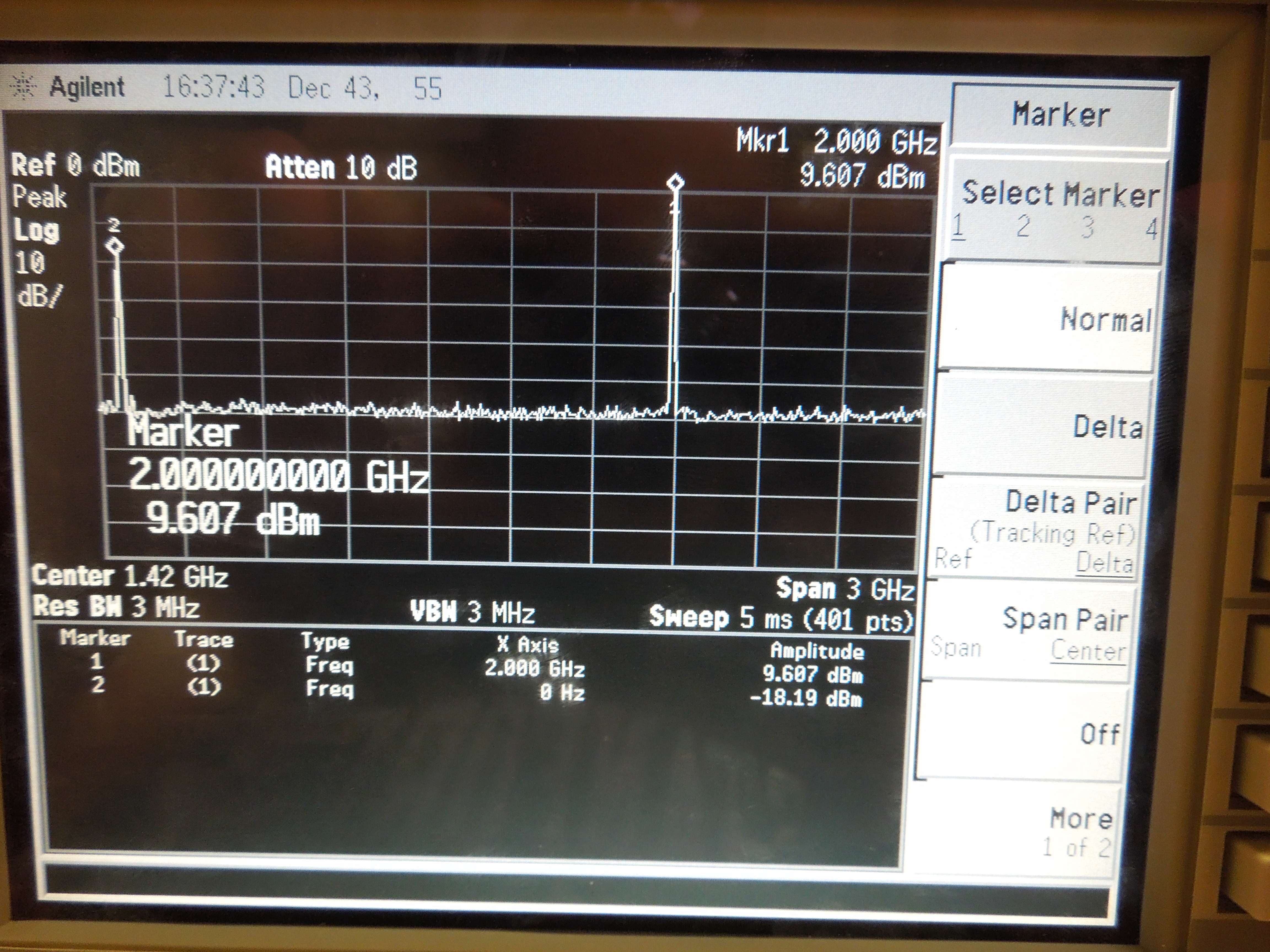
Below is a measured Digital Buffer output signal when the input signal is 2 GHz
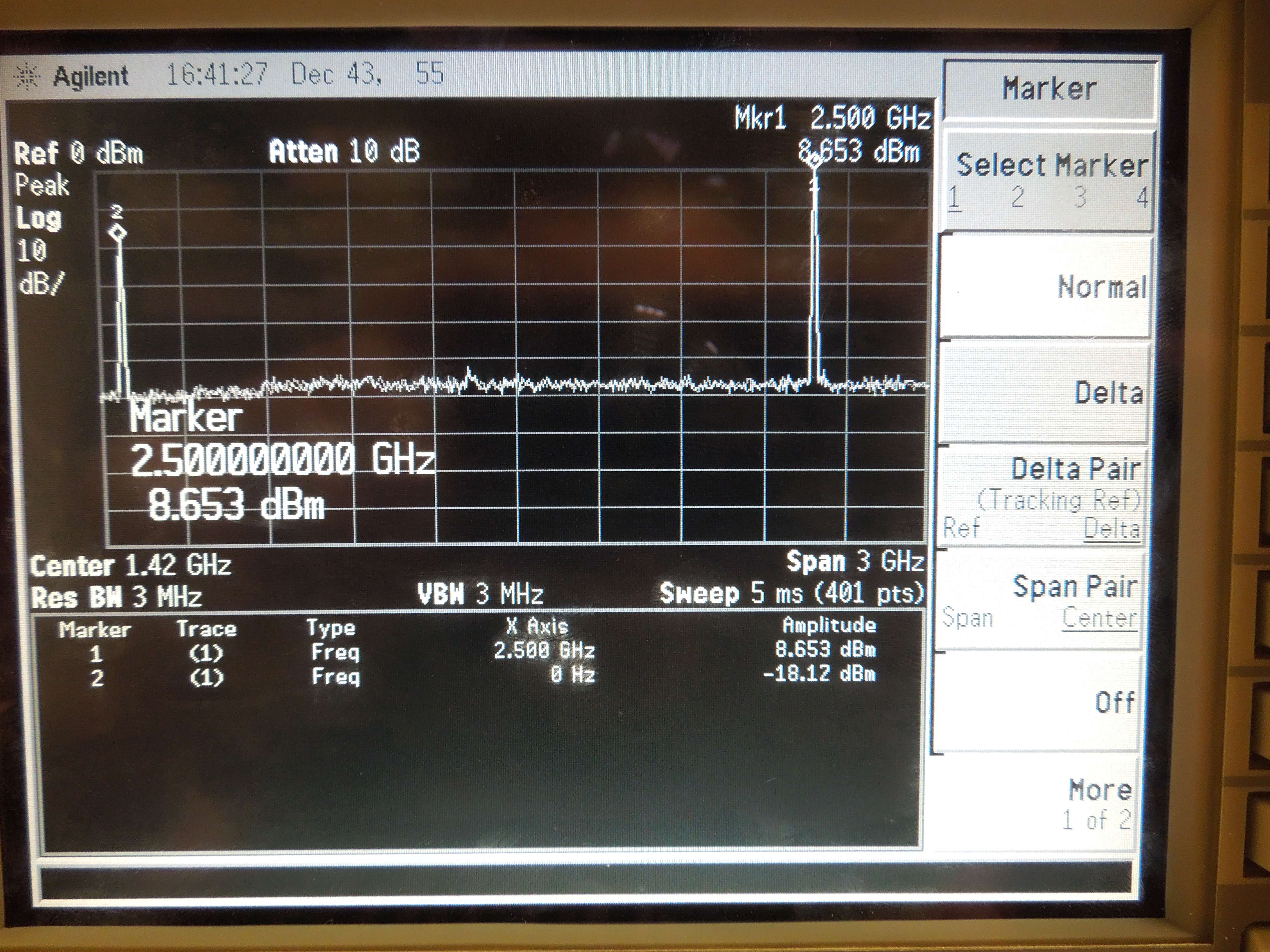
Below is a measured Digital Buffer output signal when the input signal is 2.5 GHz
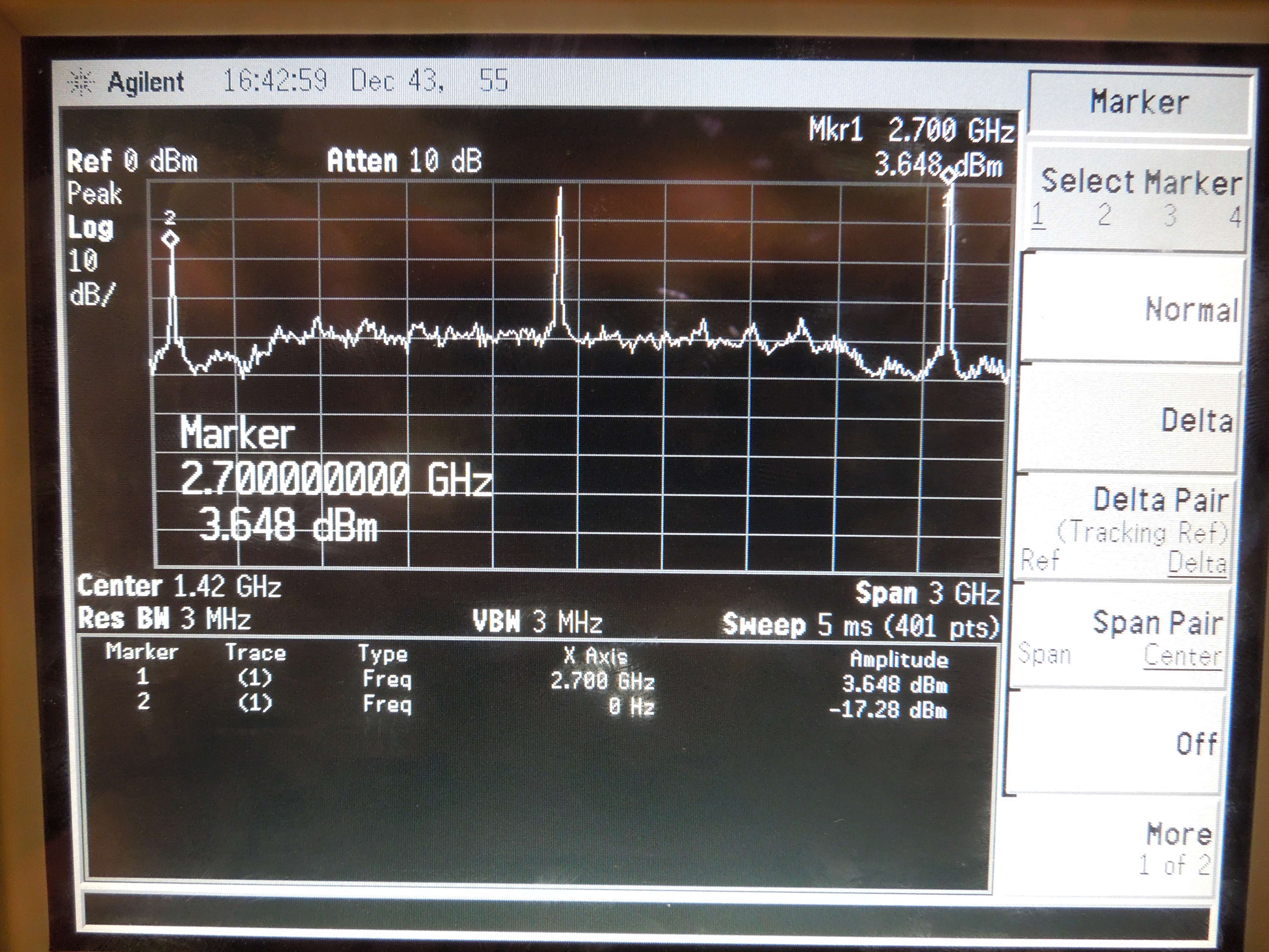
Below is a measured Digital Buffer output signal when the input signal is 2.7 GHz
Below is a measured Digital Buffer output signal when the input signal is 2.9 GHz
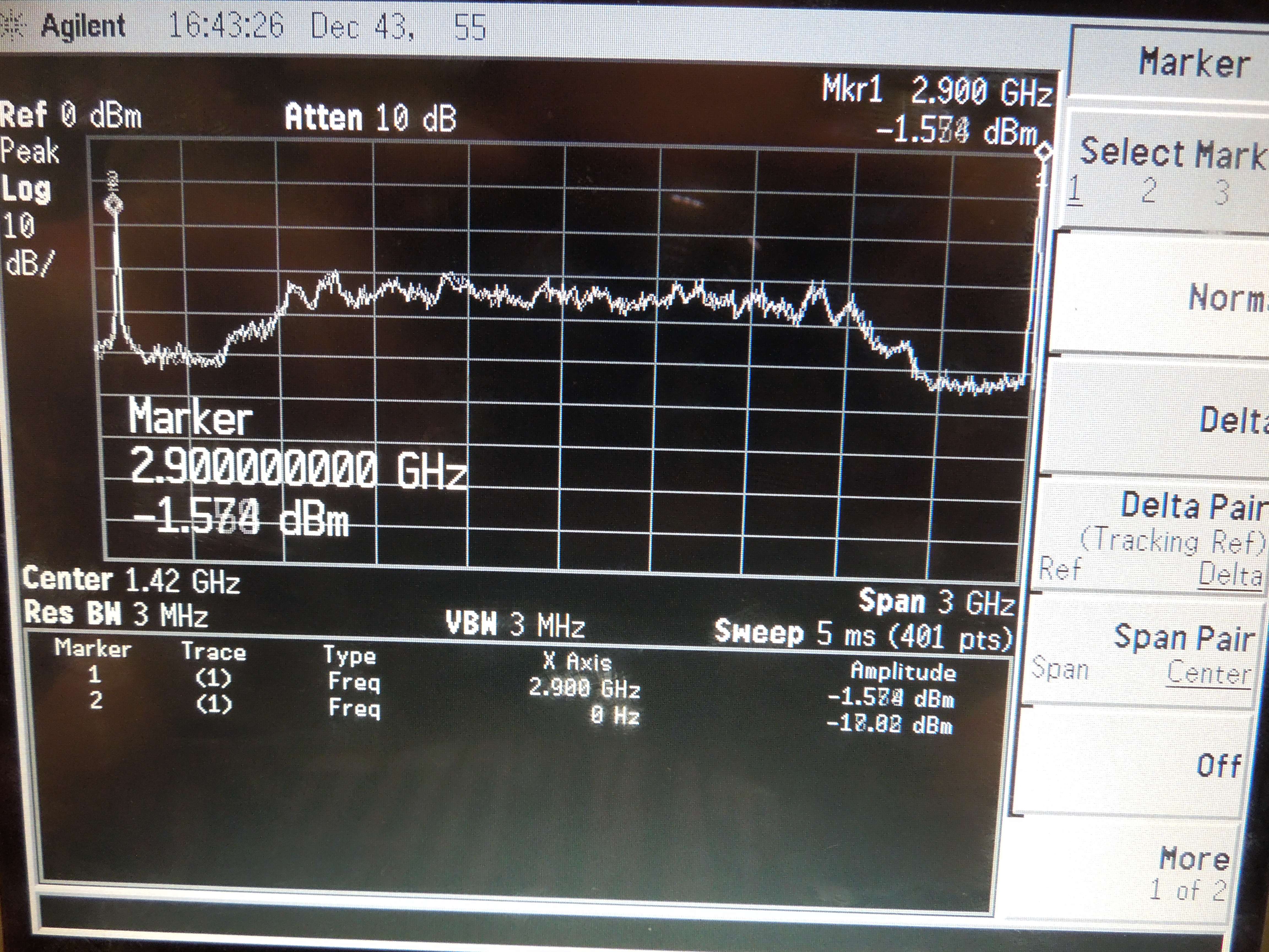
That is pretty cool. At 2.5 GHz I can still observe 8.65 dBm amplitude signal at the output. That is not bad at all. Things start getting nasty at 2.7 GHz, the amplitude drops significantly and spectrum starts getting dirtier with additional signal harmonic. At 2.9 GHz it gets even worse. But up to 2.5 GHz it works just great. Impressive.
I must also note that even though I got maximum reasonable result for Digital Buffer performance at 2.5 GHz it does not mean that the buffer itself is failing. I did not use the expencive PCB process, controlled impedance option and expencive high quality SMA connectors, it all presented additional loss and impedance mismatch, all of those factors are affecting the signal performance. I might later design Rogers type PCB which has very low signal loss and just test out just the Digital Buffer performance again. In any case, the results so far seem not bad.
The first IBM 180nm CMRF7SF test driving for me was successful! Time to move on, and design some more cool circuits! I will be using the frame I designed for this test chip as well as ESD protection solution I selected, since it all proven to be working now.

